Microfluidic chip based on dielectric electrophoresis and preparation method and application thereof

A technology of microfluidic chips and dielectrophoresis, applied in biochemical equipment and methods, methods for stress-stimulated microbial growth, chemical instruments and methods, etc., can solve problems such as the troublesome preparation of import and export in the packaging process, and affect the efficiency of chip pairing

Pending Publication Date: 2017-10-20
SOUTH UNIVERSITY OF SCIENCE AND TECHNOLOGY OF CHINA
View PDF7 Cites 18 Cited by
  • Summary
  • Abstract
  • Description
  • Claims
  • Application Information

AI Technical Summary

Problems solved by technology

[0005] The current high-throughput cell paired microfluidic chip based on the DEP method uses ITO electrodes at the top and microelectrodes at the bottom to generate DEP. The disadvantages of this structure are: (1) Polydimethylsiloxane PDMS is the most commonly used material for the preparation of microfluidic channels in microfluidic chips. It is easy to package with the chip, and the inlet and outlet of the chip can be prepared on the PDMS through a simple puncher, while the ITO electrode is in the At the top, the encapsulation process and the preparation of the inlet and outlet are more troublesome; (2) The process of DEP capturing cells is to apply an AC signal between the electrodes to generate a non-uniform electric field, which leads to the directional movement of the cells. During the pairing process, ITO acts as a The common electrode for two types of cell capture, when capturing the first type of cell, due to the effect of the induced electric field, the position used to capture the other type of cell will also be occupied by the first type of cell, which affects the pairing efficiency of the chip

Method used


Image

  • Microfluidic chip based on dielectric electrophoresis and preparation method and application thereof
  • Microfluidic chip based on dielectric electrophoresis and preparation method and application thereof
  • Microfluidic chip based on dielectric electrophoresis and preparation method and application thereof

Examples


Embodiment 1

[0079] Example 1: Dielectrophoresis-based microfluidic chip

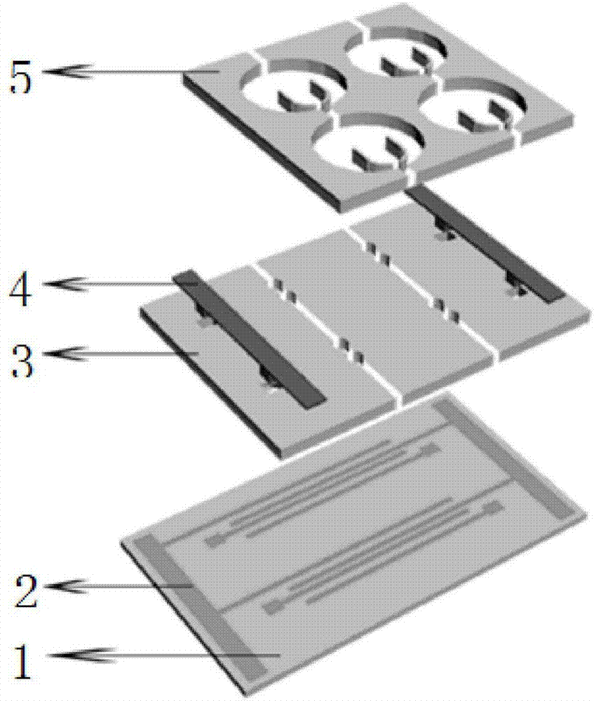
[0080] Such as Figure 6 Shown is a schematic diagram of the microfluidic chip based on dielectrophoresis described in the embodiment of the present invention. The specific structure of the microfluidic chip is as follows Figure 1-5 As shown, the microfluidic chip includes a planar chip 16 at the bottom and a microfluidic channel 13 at the top, and the planar chip has a four-layer structure stacked in sequence;

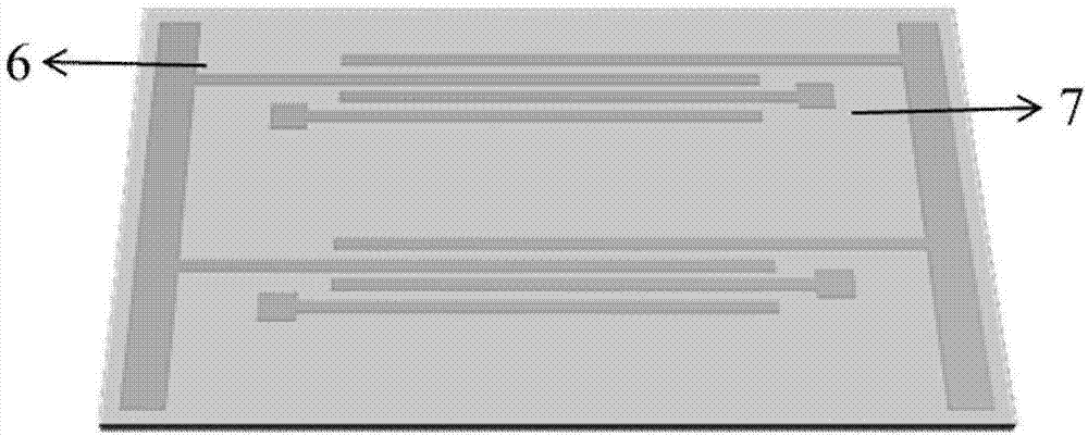
[0081] The first layer structure 1 of the planar chip includes ITO electrodes on the glass substrate, the ITO electrodes are interdigital electrodes 2, the number of the interdigital electrodes 2 is 2-10, and the width of the interdigital electrodes 2 is 10-30 μm, the distance between two electrodes in the interdigital electrodes 6 is 3-10 μm, and the distance between the interdigital electrodes 6 and 7 is 5-50 μm;

[0082] The second layer structure 3 of the planar chip is SU-8 negative glue, the second...

Embodiment 2

[0096] Example 2: Dielectrophoresis-based microfluidic chip

[0097] The microfluidic chip includes a planar chip 16 at the bottom and a microfluidic channel 13 at the top, and the planar chip has a four-layer structure stacked in sequence;

[0098] The first layer structure 1 of the planar chip includes ITO electrodes on a glass substrate, the ITO electrodes are interdigital electrodes 2, the number of the interdigital electrodes 2 is 2, and the width of the interdigital electrodes 2 is 20 μm , the distance between two electrodes in the interdigitated electrodes 6 is 6 μm, and the distance between the interdigitated electrodes 6 and 7 is 10 μm;

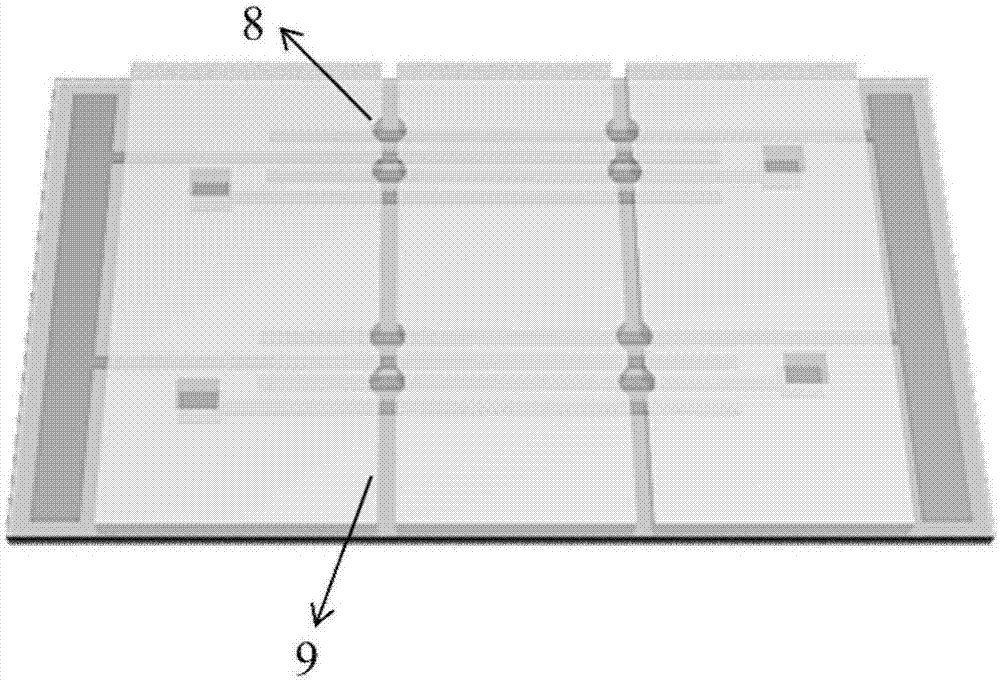
[0099] The second layer structure 3 of the planar chip is SU-8 negative glue, the second layer structure 3 shown includes a microcavity array 8 for cell capture, the diameter of the microcavity array 8 is 20 μm, and the microcavity The depth of the array 8 is 10 μm;

[0100] The third layer structure 4 of the planar chip includes a...

Embodiment 3

[0107] Example 3: Capture and pairing of cells

[0108] The microfluidic chip based on dielectrophoresis described in Example 2 is used to capture and pair cells, and the specific steps are as follows:

[0109] 1) Prepare two fluorescently labeled cell dispersions of different colors: stain the cells with two fluorescently labeled dyes, and then disperse the two kinds of cells emitting red light and green light in a low-conductivity buffer to obtain 2×10 6 / mL cell concentration of the dispersion;

[0110] 2) Put the green fluorescent cell dispersion liquid in the sampling flow channel 14 of the micro flow channel 13 on the microfluidic chip, with a flow rate of 10 μL / min, generate a non-uniform electric field between the interdigital electrodes 6 applying a sinusoidal AC signal, so that Under the action of positive dielectrophoretic force, the cells are captured into the microcavity array 8 on one side, captured for 3-5 minutes, and the excess cells are washed away with the ...


PUM

PropertyMeasurementUnit
diameteraaaaaaaaaa
depthaaaaaaaaaa
thicknessaaaaaaaaaa

Abstract

The invention relates to a microfluidic chip based on dielectric electrophoresis and a preparation method and application thereof, the microfluidic chip includes a planar chip (16) at the bottom and a micro flowing channel (13) at the top, the planar chip comprises four layers of structures which are in turn overlapped; the first layer structure(1) of the planar chip includes an electrode on a glass substrate, the electrode is an interdigital electrode (2); the second layer structure (3) of the planar chip includes a micro cavity array (8); the third layer structure (4) of the planar chip includes a conductive layer (10); the fourth layer structure (5) of the planar chip includes a micro cavity array (12) and a micro baffle (11) in the micro cavity array; the second layer structure (3) and the fourth layer structure (5) include micro flowing channels (9). The microfluidic chip can achieve high throughput single cell capture and pairing.

Description

technical field [0001] The invention belongs to the technical field of single cell capture and pairing, and relates to a dielectrophoresis-based microfluidic chip and its preparation method and application. Background technique [0002] Cell fusion, also known as cell hybridization, is a process in which two or more homologous or heterologous cells form hybrid cells under in vitro conditions by induction and culture. At present, it has become an important means in the research of modern bioengineering technology. Cell fusion technology has a wide range of applications in genetics, immunomedicine, developmental biology, drug or gene delivery, hybrid breeding and other research fields. Accurate single cell capture and pairing is the prerequisite for cell fusion research, so it is necessary to design and construct an effective single cell capture and pairing experimental platform. [0003] Dielectrophoresis (Dielectrophoresis, DEP) is a technique for manipulating particles ac...

Claims


Application Information

Patent Timeline
Patent Type & Authority Applications(China)
IPC IPC(8): C12M1/42C12M1/00C12N13/00B01L3/00
CPCC12M47/04C12N13/00B01L3/502707B01L3/50273B01L2200/12B01L2200/10B01L2300/08
Inventor 程鑫吴春卉陈日飞刘羽姜有为
Owner SOUTH UNIVERSITY OF SCIENCE AND TECHNOLOGY OF CHINA
Why Eureka
Try Eureka