Silicon carbide VDMOS device and manufacturing method thereof

A technology of silicon carbide and silicon carbide regions, which is applied in the manufacture of semiconductor/solid-state devices, semiconductor devices, electrical components, etc., can solve the problems of large forward voltage drop, unfavorable promotion of silicon carbide VDMOS devices, and rising system costs

Active Publication Date: 2017-10-20
HANGZHOU SILICON-MAGIC SEMICON TECH CO LTD
View PDF6 Cites 18 Cited by
  • Summary
  • Abstract
  • Description
  • Claims
  • Application Information

AI Technical Summary

Problems solved by technology

Silicon carbide VDMOS devices generally need to work together with an anti-parallel diode in traditional inverter circuits, chopper circuits and other circuit applications. There are usually the following two methods: one is: directly use the device Pbase, N-region and N+ lining The parasitic PIN diode formed at the bottom; due to the junction voltage drop of about 3V at the silicon carbide PN junction, if the PIN diode is used directly, it will lead to a large forward conduction voltage drop, power loss and low circuit application efficiency, which not only This leads to reliability problems caused by device heating, and attention should also be paid to the waste of energy resources; the second is to use a fast ...

Method used


Image

  • Silicon carbide VDMOS device and manufacturing method thereof
  • Silicon carbide VDMOS device and manufacturing method thereof
  • Silicon carbide VDMOS device and manufacturing method thereof

Examples


Embodiment 1

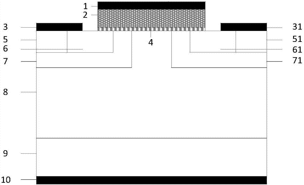
[0104] A kind of silicon carbide VDMOS device provided by the present invention, the cell structure of its basic structure is as follows figure 2 shown. It includes a metal drain electrode 10 arranged sequentially from bottom to top with a thickness of about 0.5-6 μm and a doping concentration of 1×10 18 cm -3 ~1×10 19 cm -3 , N with a thickness of 50-200 μm + The substrate 9 has a thickness of 15-18 μm and a doping concentration of about 1×10 15 cm -3 ~5×10 16 cm -3 N - Epitaxial layer 8; above the N- epitaxial layer 8 has a doping concentration of 1×10 17 ~7×10 17 cm -3 1. Implant the first Pbase region 7 with a depth of about 0.5-1 μm, and the other end of the upper layer has a second Pbase region 71 with the same parameters; the first Pbase region 7 has mutually independent doping concentrations of 1×10 19 ~1×10 20 cm -3 , implanting the first N with a depth of about 0.3-0.5 μm + The source region 6 and the doping concentration are about 3×10 19 ~1×10 20 c...

Embodiment 2

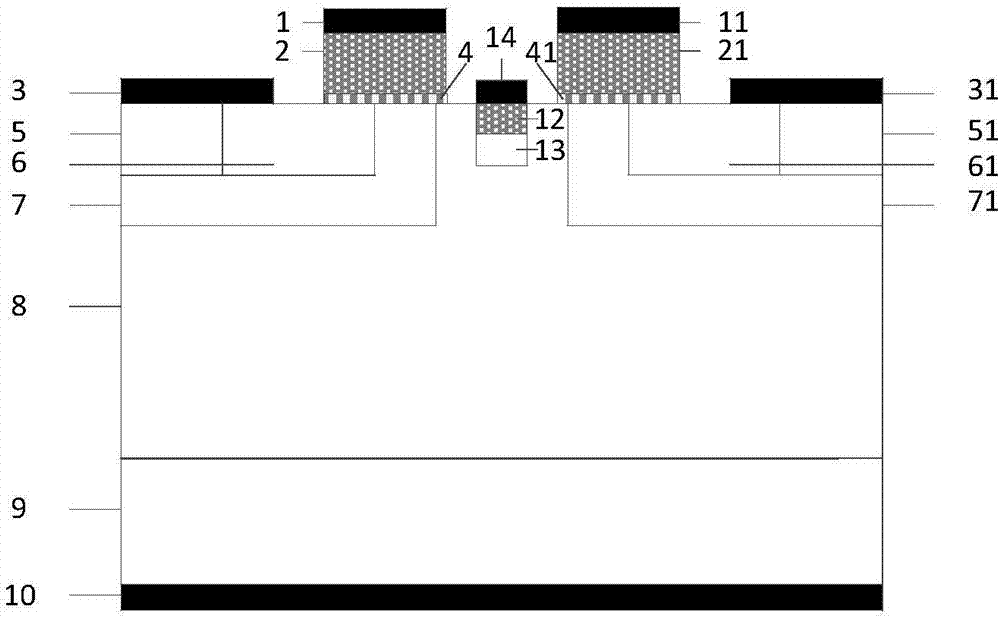
[0106] like image 3 As shown, except that the P-type silicon carbide region 13 is replaced by a dielectric layer 15 with a thickness of 0.02-0.50 μm, the rest of the structure of this embodiment is the same as that of Embodiment 1. Compared with Example 1, the dielectric layer 15 is able to P + The polysilicon layer 12 plays the role of electric field shielding and protection, thereby improving the breakdown voltage and reliability of the device, and reducing the reverse leakage current.

Embodiment 3

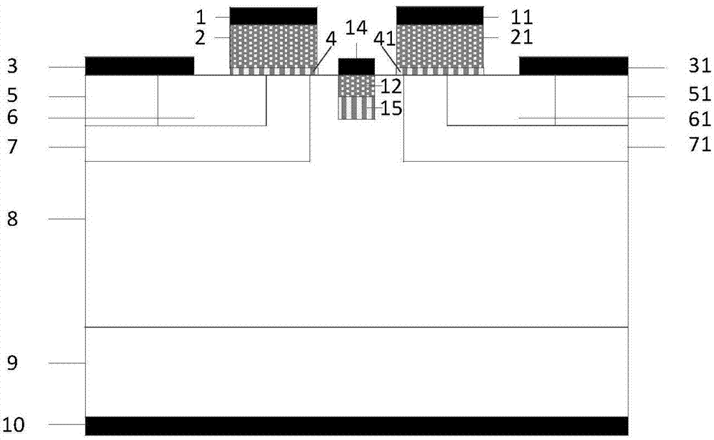
[0108] like Figure 4 As shown, except that the width of the P-type silicon carbide region 13 is larger than P + The width of the polysilicon layer 12 and the P-type silicon carbide region 13 in N - Except for the depth inside the epitaxial layer 8 , the rest of the structure of this embodiment is the same as that of Embodiment 1.

[0109] Compared with Embodiment 1, this embodiment further improves the electric field shielding effect of the P-type silicon carbide region 13, further improves the breakdown voltage and reliability of the device, and reduces the reverse leakage current.


PUM

PropertyMeasurementUnit
Thicknessaaaaaaaaaa
Thicknessaaaaaaaaaa

Abstract

The invention discloses a silicon carbide VDMOS device and manufacturing method thereof, and belongs to the technical field of power semiconductors. A trench is etched on a JFET region surface of a traditional silicon carbide VDMOS device, P type doping is introduced into the bottom of the trench, and at the same time, a polycrystalline silicon layer is formed in the trench, so that the polycrystalline silicon layer and a side wall of the trench are in contact to form a Si/SiC heterojunction. A diode is integrated in the device, and the device has the advantages of low conduction voltage drop, fast switching speed and good reverse recovery characteristic in a diode working mode, and has the advantages of high breakdown voltage, small grid capacitance and fast switching speed in an MOS working mode. The proposed device structure optimizes application of the device in the field of inverter circuits, chopper circuits and the like, and has the advantage that the process is simple, and is compatible with a traditional silicon carbide VDMOS device process.

Description

technical field [0001] The invention belongs to the technical field of power semiconductors, and in particular relates to a silicon carbide VDMOS device and a manufacturing method thereof. Background technique [0002] Since the beginning of the 21st century, the world's energy production and consumption are still dominated by fossil energy, and fossil energy will remain the energy basis for human survival and development for a relatively long period of time. However, fossil energy will eventually be exhausted, and it is easy to cause environmental pollution problems, and the resulting problems of environment and sustainable development are difficult problems that human beings must face. Therefore, as an important energy source that can be used by human beings - electric energy, the improvement of its efficiency is an important solution to the world's energy problems. [0003] The power system is a necessary way for human beings to use electric energy and improve the effici...

Claims


Application Information

Patent Timeline
IPC IPC(8): H01L29/78H01L29/16H01L29/06H01L21/336
CPCH01L29/0684H01L29/1608H01L29/66068H01L29/7802H01L29/7804H01L29/165
Inventor 张金平邹华刘竞秀李泽宏任敏张波
Owner HANGZHOU SILICON-MAGIC SEMICON TECH CO LTD
Why Eureka
Try Eureka