A kind of sensor chip and preparation method thereof

A sensor chip, chip technology, applied in the direction of scattering characteristics measurement, etc., to achieve the effect of abundant quantity, good response signal and simple method

Inactive Publication Date: 2019-09-20
中国人民解放军92232部队 +1
View PDF4 Cites 0 Cited by
  • Summary
  • Abstract
  • Description
  • Claims
  • Application Information

AI Technical Summary

Problems solved by technology

Nanoparticles have a high specific surface area and can be used to solve the above problems, but how to effectively immobilize abundant nanoparticles to the sensor surface is still a hot issue

Method used


Image

  • A kind of sensor chip and preparation method thereof
  • A kind of sensor chip and preparation method thereof
  • A kind of sensor chip and preparation method thereof

Examples


Embodiment 1

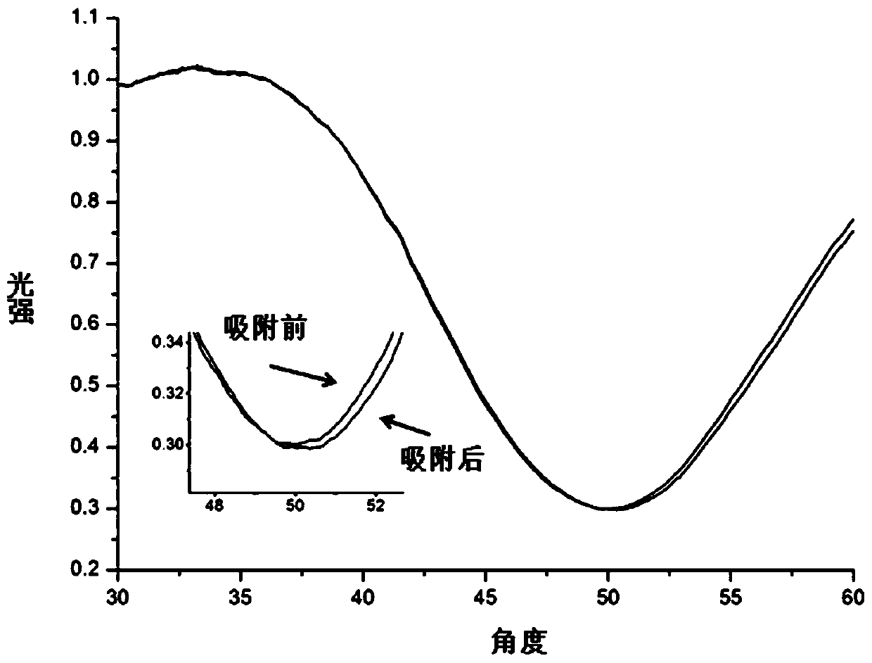
[0042] Such as figure 1 As shown, a sensor chip is composed of a glass substrate 1, a metal film 2, a self-assembled film 3 and a composite film 4 of metal oxide and polymer from bottom to top in sequence. The specific preparation steps of the sensor chip are as follows:

[0043] Step 1. Coating a metal film 2 with a thickness of 49 nm on the glass substrate 1 by vacuum evaporation;

[0044] Step 2. Place the glass substrate 1 after the vapor-deposited metal film 2 in allyl mercaptan with a concentration of 1mmol / L, and after standing still for 24h, take out the glass substrate 1 from the allyl mercaptan, and use Rinse with absolute ethanol and dry with high-purity nitrogen to form a self-assembled film 3 on the metal film 2;

[0045] Step 3. Disperse the titanium dioxide powder into distilled water and ultrasonically mix to obtain a concentration of 1×10 -6 mol / L suspension solution;

[0046] Step 4. Mix 0.0355g of acrylamide, 0.0062g of N,N'-methylenebisacrylamide and 950...

Embodiment 2

[0051] A sensor chip consists of a glass substrate 1, a metal film 2, a self-assembled film 3, and a composite film 4 of metal oxide and polymer from bottom to top. The specific preparation steps of the sensor chip are as follows:

[0052] Step 1. Coating a metal film 2 with a thickness of 45 nm on the glass substrate 1 by vacuum evaporation;

[0053] Step 2. Place the glass substrate 1 after the vapor-deposited metal film 2 in mercaptoethylamine with a concentration of 0.1mmol / L. Rinse and dry with high-purity nitrogen to form a self-assembled film 3 on the metal film 2;

[0054] Step 3. Disperse the titanium dioxide powder into distilled water and ultrasonically mix to obtain a concentration of 1×10 -7 mol / L suspension solution;

[0055] Step 4. Mix 0.0086 g of methacrylic acid, 0.0344 g of ethylene glycol dimethacrylate, and 900 μL of acetonitrile solution containing 0.002 g of azobisisobutyronitrile, and ultrasonically degas for 10 minutes to obtain a mixed solution I; ...


PUM

PropertyMeasurementUnit
particle diameteraaaaaaaaaa
thicknessaaaaaaaaaa
thicknessaaaaaaaaaa

Abstract

The invention relates to a sensor chip and a manufacturing method thereof, and belongs to the technical field of designing and manufacturing of surface plasma resonance sensor chips. The chip adopts a composite structure formed by a glass substrate, a metallic film, a self-assembly film, and a metallic oxide and polymer composite thin film, in sequential arrangement from bottom to top; and nanometer metallic oxide is successfully fixed to the surface of the sensor chip by a polymer embedding method, so that the detection range of objective gas is effectively enlarged, and the sensitivity of the objective gas is effectively improved. The method disclosed by the invention is simple, the manufactured sensor chip has high sensitivity on sulphur dioxide, detection requirements under room temperature condition are met, and the sensor chip has favorable response signals within 5 ppm-40 ppm.

Description

technical field [0001] The invention relates to a sensor chip and a preparation method thereof, belonging to the technical field of surface plasmon resonance (Surface plasmon resonance, SPR) sensor chip design and preparation. Background technique [0002] In the atmosphere, sulfur dioxide will oxidize to form sulfate aerosols, which are important precursors of environmental acidification. When the concentration of sulfur dioxide in the atmosphere reaches 0.21ppm, it can increase the incidence of respiratory diseases, so there is an urgent need for tools for real-time monitoring of the concentration of sulfur dioxide in the environment. At present, the sensors for sulfur dioxide gas are mostly electrochemical sensors but few optical sensors. [0003] As an important representative of optical sensors, surface plasmon resonance sensors can provide online real-time monitoring data, providing an effective tool for real-time monitoring of harmful gases in the environment. Surfa...

Claims


Application Information

Patent Timeline
Patent Type & Authority Patents(China)
IPC IPC(8): G01N21/55
Inventor 张鹏韩守鹏韦天新孟祥尧吴小兵张炜许杰杨振宇李卉王洋
Owner 中国人民解放军92232部队
Why Eureka
Try Eureka