Cr-doped heterojunction spin field effect transistor and preparation method thereof

A field effect transistor and heterojunction technology, which is applied in semiconductor devices, electrical components, circuits, etc., can solve the problem that the efficiency of spin injection is only a few percent, so as to improve the efficiency of spin injection and reception, and simplify the manufacture. , the effect of optimizing the spin polarizability

Active Publication Date: 2017-12-01
XIDIAN UNIV
View PDF8 Cites 2 Cited by
  • Summary
  • Abstract
  • Description
  • Claims
  • Application Information

AI Technical Summary

Problems solved by technology

[0004] However, the general spin field effect transistor injects spin electrons into semiconductors by ferromagnetic materials, and the efficiency of spin inje

Method used


Image

  • Cr-doped heterojunction spin field effect transistor and preparation method thereof
  • Cr-doped heterojunction spin field effect transistor and preparation method thereof
  • Cr-doped heterojunction spin field effect transistor and preparation method thereof

Examples


Embodiment 1

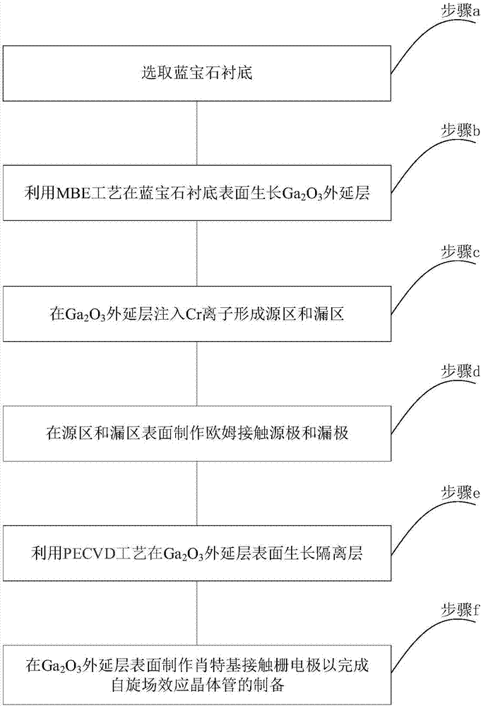
[0040] See figure 1 , figure 1 A flow chart of a method for preparing a Cr-doped heterojunction spin field effect transistor provided in an embodiment of the present invention, wherein the preparation method includes:

[0041] (a) select a sapphire substrate;

[0042] (b) Growth of Ga on the surface of sapphire substrate by MBE process 2 o 3 epitaxial layer;

[0043](c) in Ga 2 o 3 The epitaxial layer is implanted with Cr ions to form source and drain regions;

[0044] (d) making ohmic contact source and drain on the surface of source region and drain region;

[0045] (e) Ga 2 o 3 An isolation layer is grown on the surface of the epitaxial layer;

[0046] (f) in Ga 2 o 3 A schottky contact gate electrode is made on the surface of the epitaxial layer to complete the preparation of the spin field effect transistor.

[0047] Among them, Ga 2 o 3 As a wide bandgap semiconductor, its bandgap can reach 4.9ev, while the existing SiC material has a bandgap of only 3ev; ...

Embodiment 2

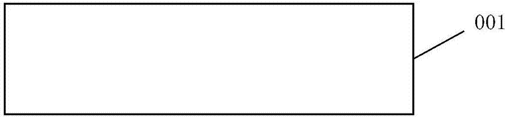
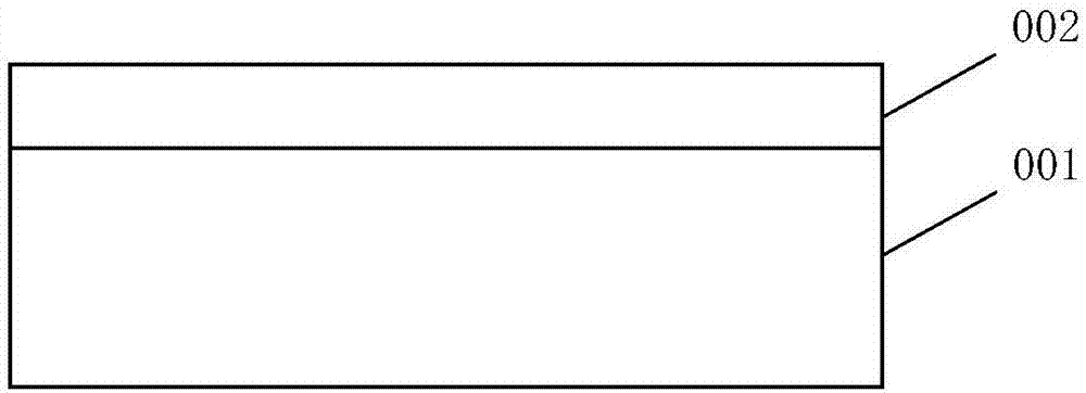
[0059] Please refer to Figure 2a-Figure 2g , Figure 2a-Figure 2g A schematic diagram of the preparation process of a Cr-doped heterojunction spin field effect transistor provided by the embodiment of the present invention, the preparation method includes the following steps:

[0060] Step 1, such as Figure 2a As shown, the sapphire substrate 001 was selected, and the sapphire substrate was ultrasonically cleaned using acetone, absolute ethanol and deionized water in sequence.

[0061] Step 2, such as Figure 2b As shown, lightly doped Ga with a thickness of 0.4-0.6 μm was grown on the surface of sapphire substrate by MBE 2 o 3 Epitaxial layer 002, N-type doping concentration is 1×10 14 -1×10 16 cm -3 ; The evaporation source material is high-purity elemental metal Ga, the mass fraction is 99.99999%, the growth temperature is 940°C, the power of the radio frequency source is 300W, and the pressure is 1.5×10 -5 Torr;

[0062] Step 3, such as Figure 2c As shown, in ...

Embodiment 3

[0074] Please refer to image 3 , image 3 A schematic structural diagram of a Cr-doped heterojunction spin field effect transistor provided by an embodiment of the present invention. The spin field effect transistor adopts the above-mentioned as Figure 2a-Figure 2g prepared as indicated.

[0075] Specifically, the spin field effect transistor includes: a sapphire substrate 301, a Ga 2 o 3 Epitaxial layer 302, Ga 2 o 3 Source region 303, Ga 2 o 3 Drain region 304 , source 305 , drain 306 , isolation layer 307 , Schottky contact gate electrode 308 .

[0076] Among them, Ga 2 o 3 source region 303 and Ga 2 o 3 The drain region 304 is made of Ga 2 o 3 The epitaxial layer 302 is formed by selectively implanting Cr ions six times.

[0077] Preferably, Ga 2 o 3 The epitaxial layer 302 has an N-type doping concentration of 1×10 14 -1×10 16 cm -3 , Ga with a point-defect structure with a thickness of 0.4–0.6 μm 2 o 3 Material.

[0078] Preferably, the isolation...


PUM

PropertyMeasurementUnit
Thicknessaaaaaaaaaa
Widthaaaaaaaaaa
Thicknessaaaaaaaaaa

Abstract

The invention relates to a Cr-doped heterojunction spin field effect transistor and a preparation method thereof. The preparation method comprises: selecting a sapphire substrate; growing a Ga2O3 epitaxial layer on the surface of the sapphire substrate by employing a MBE process; injecting Cr ions into the Ga2O3 epitaxial layer to form a source region and a drain region; fabricating an ohmic contact source electrode and a drain electrode on the surfaces of the source region and the drain region; growing a separating layer on the surface of the Ga2O3 epitaxial layer by employing a PECVD process; and fabricating a Schottky contact gate electrode on the surface of the Ga2O3 epitaxial layer to accomplish the preparation of the spin field effect transistor. According to the Cr-doped heterojunction spin field effect transistor and the preparation method, the doping concentration and the defect concentration in source-drain materials can be changed through adjustment of the dosage of ion implantation and the annealing time so that the spin polarizability of the materials at a room temperature is optimized.

Description

technical field [0001] The invention belongs to the technical field of semiconductor device preparation, in particular to a method for doping Ga with Cr ions using paired point defects. 2 o 3 Fabrication of a heterojunction high electron mobility spin field effect transistor with source-drain injection to receive spin-polarized electrons and a fabrication method. Background technique [0002] With the rapid update of modern electronic technology, the development of traditional electronic devices has severely restricted the development of microelectronics science in terms of scale integration and computing speed. The emerging spintronics aims to conveniently regulate the spin of electrons, opening up a new field of information storage and transmission by using spin of electrons, which has caused research in multiple scientific fields such as physics, materials science and electronic information science. common concerns and broad interests of readers. [0003] In recent yea...

Claims


Application Information

Patent Timeline
IPC IPC(8): H01L29/66H01L29/778H01L29/812
CPCH01L29/66068H01L29/66984H01L29/7786H01L29/812
Inventor 贾仁需杨宇元磊张玉明彭博
Owner XIDIAN UNIV
Why Eureka
Try Eureka