
Silicon carbide semiconductor device and method for manufacturing same

A semiconductor and silicon carbide technology, which is applied to trench gate type silicon carbide semiconductor devices and their manufacturing fields, can solve the problems of high dielectric breakdown strength, electric field concentration, damage to gate insulating films, etc., so as to improve the avalanche breakdown voltage. , The effect of high device withstand voltage

Active Publication Date: 2017-12-01
MITSUBISHI ELECTRIC CORP
View PDF6 Cites 13 Cited by
  • Summary
  • Abstract
  • Description
  • Claims
  • Application Information

AI Technical Summary

Problems solved by technology

Especially in the case of using SiC as the semiconductor material, electric field concentration at the bottom of the trench tends to be a problem
The reason for this is that because of the high insulation breakdown strength of the semiconductor material itself, compared with the avalanche breakdown in the drift layer, the damage to the gate insulating film caused by the concentration of the electric field at the bottom of the trench is likely to occur first.

Method used


Image

  • Silicon carbide semiconductor device and method for manufacturing same
  • Silicon carbide semiconductor device and method for manufacturing same
  • Silicon carbide semiconductor device and method for manufacturing same

Examples


Embodiment approach 1

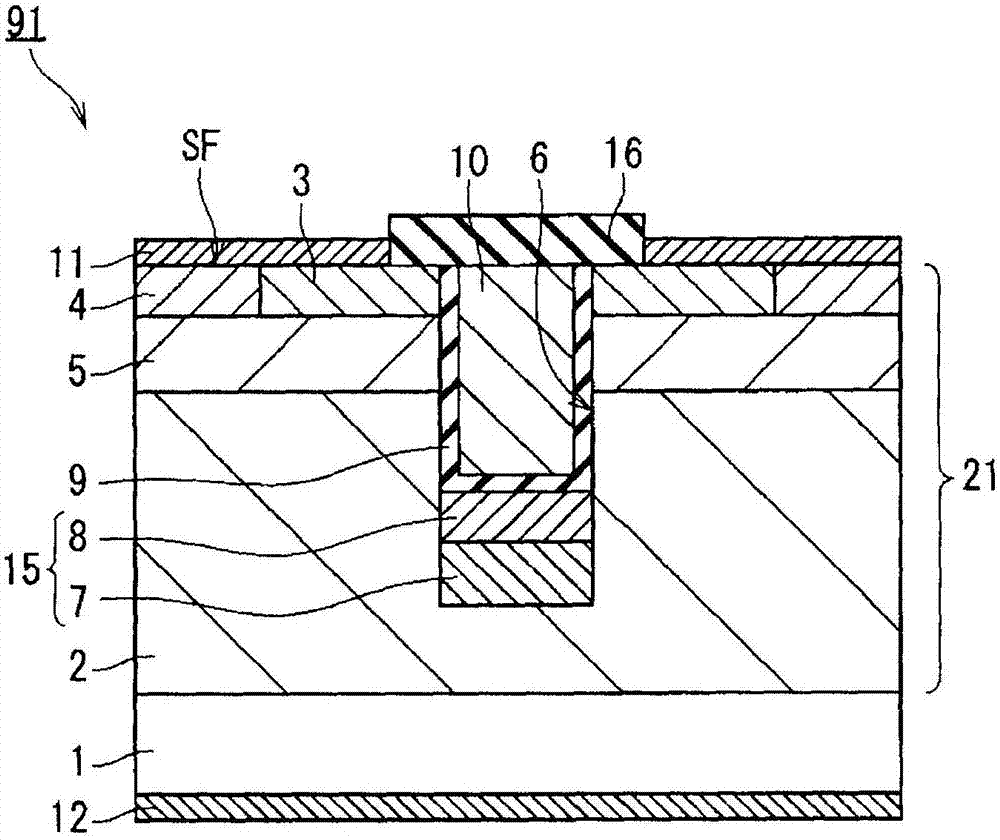
[0041] figure 1 It is a cross-sectional view schematically showing a cell structure of MOSFET 91 (silicon carbide semiconductor device) according to this embodiment. MOSFET 91 has substrate 1 (semiconductor substrate), semiconductor layer 21 , gate oxide film 9 (gate insulating film), gate electrode 10 , source electrode 11 , drain electrode 12 , and interlayer insulating film 16 .

[0042] The substrate 1 is an n-type (first conductivity type) silicon carbide semiconductor substrate. The plane orientation of the substrate 1 may be, for example, any plane orientation such as (0001) plane, (000-1) plane, or (11-20) plane. In addition, a substrate provided with an off angle (of angle) in each plane orientation may also be used.

[0043] The semiconductor layer 21 is formed of silicon carbide. The semiconductor layer 21 is an epitaxial layer on the substrate 1 . The semiconductor layer 21 has an n-type drift layer 2 provided on the substrate 1, a p-type (second conductivity t...

Embodiment approach 2

[0096] Figure 14 It is a cross-sectional view schematically showing a cell structure of MOSFET 92 (silicon carbide semiconductor device) according to this embodiment. In this embodiment, compared with Embodiment 1, the structure of trench bottom surface protection layer 15 is different. Specifically, in the trench bottom protective layer 15 of the MOSFET 92 , the width of the low-concentration protective layer 7 is smaller than the width of the high-concentration protective layer 8 . Therefore, the low-concentration protective layer 7 forms only a part of the bottom surface of the trench bottom surface protective layer 15 (in the figure, the central portion of the bottom surface), and the high-concentration protective layer 8 forms the other part of the bottom surface of the trench bottom surface protective layer 15 (in the figure). middle, both ends of the bottom surface). It should be noted that configurations other than those described above are substantially the same as...

Embodiment approach 3

[0105] Figure 16 It is a cross-sectional view schematically showing a cell structure of MOSFET 93 (silicon carbide semiconductor device) according to this embodiment. In this embodiment, compared with Embodiment 1, the structure of trench bottom surface protection layer 15 is different. Specifically, in the trench bottom protective layer 15 of the MOSFET 93 , the width of the low-concentration protective layer 7 is larger than the width of the high-concentration protective layer 8 . It should be noted that configurations other than those described above are substantially the same as those of Embodiment 1 described above, and therefore description thereof will not be repeated.

[0106] Next, a method of manufacturing MOSFET 93 will be described below.

[0107] refer to Figure 17A first drift layer 2 a (first layer) made of silicon carbide and having an n-type is formed on the substrate 1 . It should be noted that the method of forming the first drift layer 2a can be compa...


PUM


Abstract

The invention provides a silicon carbide semiconductor device and a method for manufacturing the same. According to the invention, a first-conductivity-type drift layer (2) comprises silicon carbide. A second-conductivity-type body region (5) is provided on the drift layer (2). A first-conductivity-type source region (3) is provided on the body region (5). A source electrode (11) is connected to the source region (3). A gate insulating film (9) is provided on the side surfaces and the bottom surface of a trench (6) that passes through the body region (5) and the source region (3). A gate electrode (10) is provided inside the trench (6) with the gate insulating film (9) interposed therebetween. A second-conductivity-type trench-bottom-surface protective layer (15) is provided below the bottom surface of the trench (6) within the drift layer (2), and is electrically connected to the source electrode (11). The trench-bottom-surface protective layer (15) has: a high-density protective layer (8); and a first low-density protective layer (7) provided below the high-density protective layer (8) and having a lower impurity density than the high-density protective layer (8).

Description

technical field [0001] The present invention relates to a silicon carbide semiconductor device and a manufacturing method thereof, in particular to a trench gate type silicon carbide semiconductor device and a manufacturing method thereof. Background technique [0002] Insulated gate semiconductor devices such as MOSFET (Metal Oxide Semiconductor Field Effect Transistor) and IGBT (Insulated Gate Bipolar Transistor) are widely used as power switching elements. In an insulated gate semiconductor device, a channel is formed in a body region by applying a voltage equal to or higher than a threshold voltage to a gate electrode, thereby obtaining an on state. Especially when a trench gate type semiconductor device is used, the cell pitch can be reduced by increasing the channel width density. Accordingly, it is possible to reduce the size of the device, apply it to a large current, and improve the performance of the device. [0003] On the other hand, semiconductor devices using...

Claims


Application Information

Patent Timeline
Patent Type & Authority Applications(China)
IPC IPC(8): H01L29/78H01L21/336H01L29/06H01L29/12
CPCH01L29/0623H01L29/1608H01L29/66068H01L29/7397H01L29/7813H01L21/0465H01L29/1045
Inventor 田中梨菜香川泰宏菅原胜俊三浦成久
Owner MITSUBISHI ELECTRIC CORP
Learn More