Copper indium gallium diselenide thin film solar cell back electrode and preparation method thereof

A solar cell, copper indium gallium selenide technology, applied in the direction of circuits, photovoltaic power generation, electrical components, etc., can solve problems such as the decrease in the binding force between the absorber layer and the back electrode, the impact of subsequent battery processing, and the impact on the photoelectric conversion rate of CIGS thin film batteries. Achieve the effect of avoiding reaction and ensuring stability

Pending Publication Date: 2017-12-08
蚌埠兴科玻璃有限公司 +2
View PDF9 Cites 5 Cited by
  • Summary
  • Abstract
  • Description
  • Claims
  • Application Information

AI Technical Summary

Problems solved by technology

When the substrate is soda-lime glass, during the high-temperature selenization process after depositing the copper indium gallium metal prefabricated layer or the high-temperature co-deposition process of the four elements of CIGS, the sodium in the glass diffuses through the back electrode and enters the CIGS absorber layer , but due to the large sodium content in soda-lime glass and the variation of sodium content in different glass substrates, the uncertainty of the total amount of sodium diffused into the CIGS layer will eventually lead to the uncertainty of the CIGS crystal structure, affecting the CIGS thin film The photoelectric conversion rate of the battery. When the substrate material is stainless steel or high-temperature-resistant polymer

Method used


Image

  • Copper indium gallium diselenide thin film solar cell back electrode and preparation method thereof
  • Copper indium gallium diselenide thin film solar cell back electrode and preparation method thereof

Examples


Embodiment 1

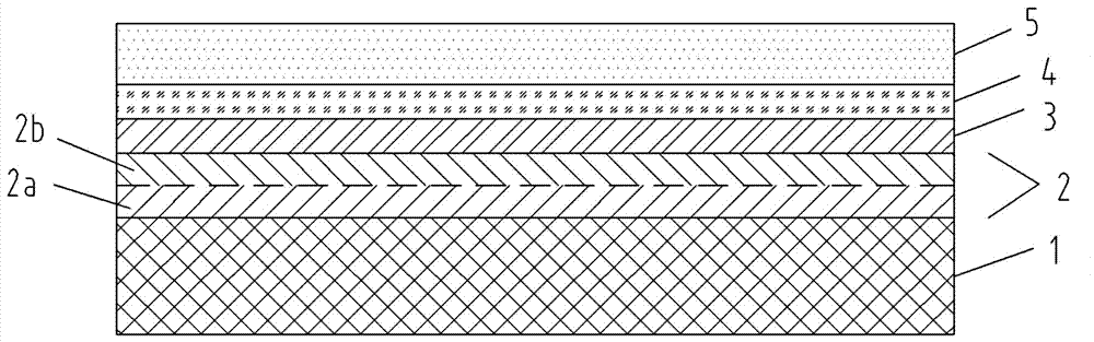
[0026] Such as figure 1 As shown, the present invention provides a back electrode of a copper indium gallium selenide thin film solar cell, including a substrate 1, a metal conductive layer 2, a barrier layer 3, a Na alloy layer 4 and an outer protective conductive layer 5 arranged in sequence from bottom to top;

[0027] Substrate 1 adopts glass substrate; Metal conductive layer 2 is wherein one or more than two kinds of Mo, W, Ta, Cu, as preferred, this embodiment adopts Mo, by Mo conductive inner layer 2a and Mo conductive outer layer 2b constitutes,

[0028] The thickness is 100-500nm in total.

[0029] The barrier layer 3 is transition metal nitride or oxynitride, titanium oxynitride is used in this embodiment; the thickness is 10-80 nm.

[0030] The Na alloy layer 4 is composed of Na and another alloy element, and the Na content in the Na alloy layer is 2 to 10% molar ratio; the thickness of the Na alloy layer 4 is 20 to 50 nm; the other in the Na alloy layer One allo...

Embodiment 2

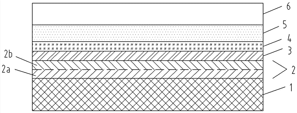
[0044] Such as figure 1As shown, the present invention provides a back electrode of a copper indium gallium selenide thin film solar cell, including a substrate 1, a metal conductive layer 2, a barrier layer 3, a Na alloy layer 4 and an outer protective conductive layer 5 arranged in sequence from bottom to top;

[0045] The substrate 1 adopts a flexible stainless steel substrate; the metal conductive layer 2 is one or more of Cr, Mo, W, Ta, Cu, as preferred, this embodiment uses Cr, Mo and Cu, and the conductive inner layer of Cr 2a is composed of MoCu alloy conductive outer layer 2b, with a total thickness of 100-500nm.

[0046] The barrier layer 3 is transition metal nitride or oxynitride, molybdenum nitride is used in this embodiment; the thickness is 10-80 nm.

[0047] The Na alloy layer 4 is composed of Na and another alloy element, and the Na content in the Na alloy layer is 2 to 10% molar ratio; the thickness of the Na alloy layer 4 is 20 to 50 nm; the other in the Na...


PUM

PropertyMeasurementUnit
Thicknessaaaaaaaaaa
Thicknessaaaaaaaaaa
Thicknessaaaaaaaaaa

Abstract

The present invention discloses a copper indium gallium diselenide (CIGS) thin film solar cell back electrode. The back electrode comprises a substrate, a metal conduction layer, a barrier layer, an Na alloy layer and an external protection conduction layer arranged in order from down to up; the barrier layer is transition metal nitride or nitric oxide; the Na alloy layer is formed by Na and another alloy element, and the Na content in the Na alloy layer is 2-10% molar ratio; the thickness of the Na alloy layer is 20-50 nm; magnetron sputtering is employed to perform deposition of each structure layer in order on the substrate for completing preparation; the Na alloy layer is taken as an Na diffusion source to provide Na required by crystal growth for the CIGS absorption layer, the barrier layer can prevent the Na from diffusion to the direction of the substrate and also prevent the impurities in the substrate from diffusion to the CIGS absorption layer to realize the accurate control of Na, and the barrier layer prevents selenium element in the deposition process from diffusion to the metal conduction layer so as to avoid reaction between the selenium and the metal conduction layer and ensure the stability of the metal conduction layer in the growth process of the CIGS absorption layer.

Description

technical field [0001] The invention relates to the technical field of thin film solar cells, in particular to a back electrode of a copper indium gallium selenium thin film solar cell with precisely controlled sodium diffusion and a preparation method thereof. Background technique [0002] In the existing solar cell technology, copper indium gallium selenide (CIGS for short) thin-film solar cell has high photoelectric conversion rate, good low-light performance, and low cost. It can be formed on a hard substrate such as glass to make a rigid Components can also be made into flexible components on flexible substrates, such as stainless steel, aluminum and high-temperature-resistant polymer materials, and are most suitable for use in building integrated photovoltaics (BIPV). It has attracted people's attention and is a very Development potential of solar cell technology. [0003] The theoretical maximum efficiency of CIGS thin-film solar cells is 33%, but the highest efficie...

Claims


Application Information

Patent Timeline
IPC IPC(8): H01L31/0224H01L31/0749
CPCH01L31/022425H01L31/0749Y02E10/541
Inventor 夏申江车兆华周建民黄海青屠友明
Owner 蚌埠兴科玻璃有限公司
Why Eureka
Try Eureka