Silicon carbide device terminal and manufacture method for the same

A manufacturing method and silicon carbide technology, which are applied in semiconductor/solid-state device manufacturing, semiconductor devices, electrical components, etc., can solve problems such as affecting the reliability of the breakdown voltage of the device, affecting the electric field distribution on the surface of the device, and being unfavorable to improve the current. The effect of improving surface electric field distribution, improving breakdown voltage and device withstand voltage performance, and reducing sensitivity

Inactive Publication Date: 2017-12-22
INST OF MICROELECTRONICS CHINESE ACAD OF SCI
View PDF4 Cites 4 Cited by
  • Summary
  • Abstract
  • Description
  • Claims
  • Application Information

AI Technical Summary

Problems solved by technology

[0005] However, due to the high surface electric field of SiC power devices, in order to improve the withstand voltage, it is necessary to reduce the surface peak electric field during device design, requiring the design of a large number of field limiting loops
Therefore, there are many factors to be considered in the design, such as the number of field limiting rings, the ring width, the distance between each field limiting ring, etc.; and the terminal with multiple field limiting rings occupies a large chip area, which is not conducive to increasing the current
However, there is a figure of merit concentration in the junction terminal extension structure and the breakdown voltage of the device is sensitive to the figure of merit concentration, so the design window is relatively small; and the junction terminal extension structure is very sensitive to the surface charge, which is easily caused by interface instability and oxide layer charge. Thus affecting the electric field distribution on the surface of the device, which in turn affects the breakdown voltage and reliability of the device

Method used


Image

  • Silicon carbide device terminal and manufacture method for the same
  • Silicon carbide device terminal and manufacture method for the same
  • Silicon carbide device terminal and manufacture method for the same

Examples


Embodiment Construction

[0031] In order to make the purpose, technical solutions and advantages of the embodiments of the present invention clearer, the technical solutions in the embodiments of the present invention will be clearly and completely described below in conjunction with the drawings in the embodiments of the present invention. Obviously, the described embodiments It is only some embodiments of the present invention, but not all embodiments. Based on the embodiments of the present invention, all other embodiments obtained by persons of ordinary skill in the art without making creative efforts belong to the protection scope of the present invention.

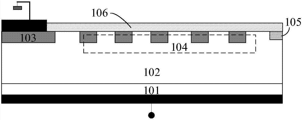
[0032] figure 1 A schematic diagram of a field limiting ring structure in the prior art is shown. As shown in the figure, the field limit ring structure includes: heavily doping a semiconductor material such as silicon carbide (SiC) wafers with Group V impurities such as nitrogen, phosphorus, and arsenic to form N + - SiC substrate 101; in ...


PUM

PropertyMeasurementUnit
thicknessaaaaaaaaaa
thicknessaaaaaaaaaa

Abstract

The invention provides a silicon carbide device terminal and a manufacture method for the same. The manufacture method for the silicon carbide device terminal comprises steps of growing an N--SiC epitaxial layer on an N+-SiC substrate, preparing a P-Sic JTE area and an N type cutoff ring in the N-epitaxial layer, wherein the a shallow groove for depositing a first passivation layer is etched in the P-Sic JTE area and the N type cutoff ring is arranged on the outer edge of a device terminal, preparing a stacking layer structure on the surface of the N-Sic epitaxial layer, wherein the stacking layer structure comprises a second passivation layer, a polycrystalline silicon field plate, a third passivation layer and a metal field plate which are stacked successively from the bottom to the top, the polycrystalline silicon field plate and the metal field plate cover a P-SiC JTE area and part of the area between the P-SiC JTE and the N type cutoff ring, the metal field plate is directly arranged on the polycrystalline silicon field plate in part of the area where is away from one side of the N type cutoff ring and the polycrystalline silicon field plate is projected toward the outer edge direction of the device terminal on one side of the N type cutoff ring. The invention also provides a terminal of a silicon carbide device. The silicon carbide device terminal and the manufacture method for the same can improve charge resistance and reliability.

Description

technical field [0001] The invention relates to the technical field of semiconductor devices, in particular to a silicon carbide device terminal and a manufacturing method thereof. Background technique [0002] Modern technology has continuously put forward higher requirements for the volume, reliability, withstand voltage and power consumption of semiconductor power devices. With the shrinking of the transistor feature size, due to the short channel effect and other physical laws and the limitation of production cost, the mainstream silicon-based materials and CMOS technology are developing to the 10nm process node and it is difficult to continue to improve. [0003] The third-generation semiconductor material silicon carbide (SiC) has a larger band gap and higher critical breakdown field strength than silicon. Compared with silicon power devices of the same withstand voltage level, SiC has higher doping concentration and more The thickness of the epitaxial layer is small,...

Claims


Application Information

Patent Timeline
Patent Type & Authority Applications(China)
IPC IPC(8): H01L29/06H01L21/336H01L29/861
Inventor 田晓丽白云杨成樾汤益丹陈宏刘新宇
Owner INST OF MICROELECTRONICS CHINESE ACAD OF SCI
Why Eureka
Try Eureka