Preparation methods of SiC device gate dielectric layer and SiC device structure

A technology of gate dielectric layer and device structure, applied in semiconductor/solid-state device manufacturing, semiconductor devices, electrical components, etc., can solve the problems of low critical breakdown strength, high thermal budget of gate dielectric layer, large leakage current, etc., to avoid C Cluster aggregation, high critical breakdown strength, and low leakage

Active Publication Date: 2017-12-29
SHANGHAI INST OF MICROSYSTEM & INFORMATION TECH CHINESE ACAD OF SCI
View PDF6 Cites 5 Cited by
  • Summary
  • Abstract
  • Description
  • Claims
  • Application Information

AI Technical Summary

Problems solved by technology

[0005] In view of the shortcomings of the prior art described above, the purpose of the present invention is to provide a method for preparing a SiC device gate dielectric layer and a SiC device structure, which is used to solve the high thermal budget and critical breakdown strength of the gate dielectric layer in the prior art Low and large leakage problems

Method used


Image

  • Preparation methods of SiC device gate dielectric layer and SiC device structure
  • Preparation methods of SiC device gate dielectric layer and SiC device structure

Examples


Embodiment 1

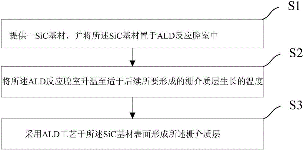
[0071] Such as figure 1 As shown, the present invention provides a method for preparing a gate dielectric layer of a SiC device, comprising the following steps:

[0072] 1) providing a SiC substrate, and placing the SiC substrate in an ALD reaction chamber;

[0073] 2) raising the temperature of the ALD reaction chamber to a temperature suitable for the subsequent growth of the gate dielectric layer to be formed;

[0074] 3) Forming the gate dielectric layer on the surface of the SiC substrate by using an ALD process.

[0075] The method for preparing the gate dielectric layer of the SiC device of the present invention will be described in detail below with reference to the accompanying drawings.

[0076] Such as figure 1 Shown in S1 in, carry out step 1), provide a SiC substrate, and described SiC substrate is placed in the ALD reaction chamber;

[0077] Specifically, the SiC base material includes but is not limited to SiC epitaxial wafers. In this embodiment, the SiC ba...

Embodiment 2

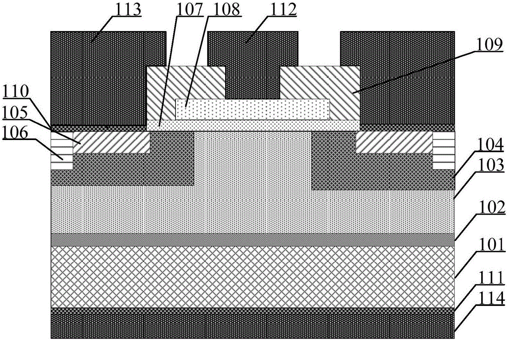
[0118] Such as figure 2 As shown, the present invention provides a method for preparing a SiC device structure, including the step of preparing a gate dielectric layer by using the method for preparing a gate dielectric layer of a SiC device as described in any one of Embodiment 1.

[0119] As an example, the method for preparing the SiC device structure includes the following steps:

[0120] 1) A heavily doped substrate of the first doping type is provided, such as a SiC substrate 101, and the substrate has a first surface and a second surface, and a lightly doped substrate of the first doping type is formed on the first surface. Doped SiC epitaxial layer 103;

[0121] 2) defining a gate structure region in the SiC epitaxial layer, and forming a second-type doped annular well region, such as a P-type well region 104, in the SiC epitaxial layer surrounding the gate structure region;

[0122] 3) Forming a heavily doped source region of the first doping type in the well regio...


PUM

PropertyMeasurementUnit
Thicknessaaaaaaaaaa
Thicknessaaaaaaaaaa

Abstract

The invention provides preparation methods of a SiC device gate dielectric layer and a SiC device structure. The preparation method of a gate dielectric layer includes the following steps: providing a SiC substrate, and placing the SiC substrate in an ALD reaction chamber; heating the ALD reaction chamber to a temperature suitable for the growth of a gate dielectric layer to be formed subsequently; and forming a gate dielectric layer on the surface of the SiC substrate through an ALD process. According to the technical scheme, Si atoms in a SiC epitaxial wafer are not consumed in the growth process of the gate dielectric layer, so that the phenomenon of C group aggregation at the interface of a gate dielectric film and SiC is avoided, and the interface property is improved. The gate dielectric layer is formed through an ALD technology, the thermal budget is low, and the device preparation process is simplified. The gate dielectric layer formed through the ALD technology has the advantages of high critical breakdown strength, low leakage and high dielectric constant. The strength of electric field introduced to the gate dielectric film can be greatly reduced, and breakdown of the gate dielectric can be avoided.

Description

technical field [0001] The invention belongs to the technical field of semiconductor technology, and in particular relates to a preparation method of a SiC device gate dielectric layer and a preparation method of a SiC device structure. Background technique [0002] Silicon carbide (SiC) material, as the third-generation wide bandgap semiconductor material, has the characteristics of high critical breakdown electric field, high thermal conductivity, high electron saturation drift rate, etc., especially in harsh environments such as high temperature or strong corrosiveness, it has great application potential , suitable for making high-temperature, high-frequency, high-power and radiation-resistant devices. The urgent need for the development of the new generation of SiC power electronic device industry will directly affect the upgrading of my country's power electronic equipment and system industry. It is urgent to carry out the layout of the SiC power electronic device indus...

Claims


Application Information

Patent Timeline
IPC IPC(8): H01L21/28H01L21/285
CPCH01L21/28158H01L21/28255H01L21/285
Inventor 程新红王谦郑理沈玲燕张栋梁顾子悦钱茹俞跃辉
Owner SHANGHAI INST OF MICROSYSTEM & INFORMATION TECH CHINESE ACAD OF SCI
Why Eureka
Try Eureka