
A kind of zinc oxide ink and its preparation method, electron transport film layer and display device

A technology of electron transport and zinc oxide, applied in chemical instruments and methods, inks, circuits, etc., can solve the problems affecting the quality of the film layer, the film layer is prone to a large number of holes, and the formation of black spots

Active Publication Date: 2020-10-30
BOE TECH GRP CO LTD
View PDF12 Cites 0 Cited by
  • Summary
  • Abstract
  • Description
  • Claims
  • Application Information

AI Technical Summary

Problems solved by technology

In the process of forming the electron transport layer by inkjet printing, the zinc oxide nanoparticles in the zinc oxide ink are easy to aggregate, resulting in the formation of black spots in the final film formation; at the same time, the zinc oxide ink is printed due to solvent volatilization Faster, resulting in a large number of holes in the printed film layer, which seriously affects the quality of the film layer

Method used


Image

  • A kind of zinc oxide ink and its preparation method, electron transport film layer and display device
  • A kind of zinc oxide ink and its preparation method, electron transport film layer and display device
  • A kind of zinc oxide ink and its preparation method, electron transport film layer and display device

Examples


Embodiment 1

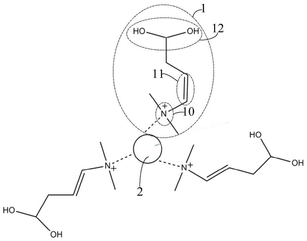
[0033] This embodiment provides a kind of zinc oxide ink, such as figure 1 As shown, it includes zinc oxide nanoparticles 2 loaded with a ligand 1, and the ligand 1 adopts an aliphatic chain with more than two carbon atoms; the ligand 1 has a crosslinkable group 11 on the side close to the coordination atom 10.

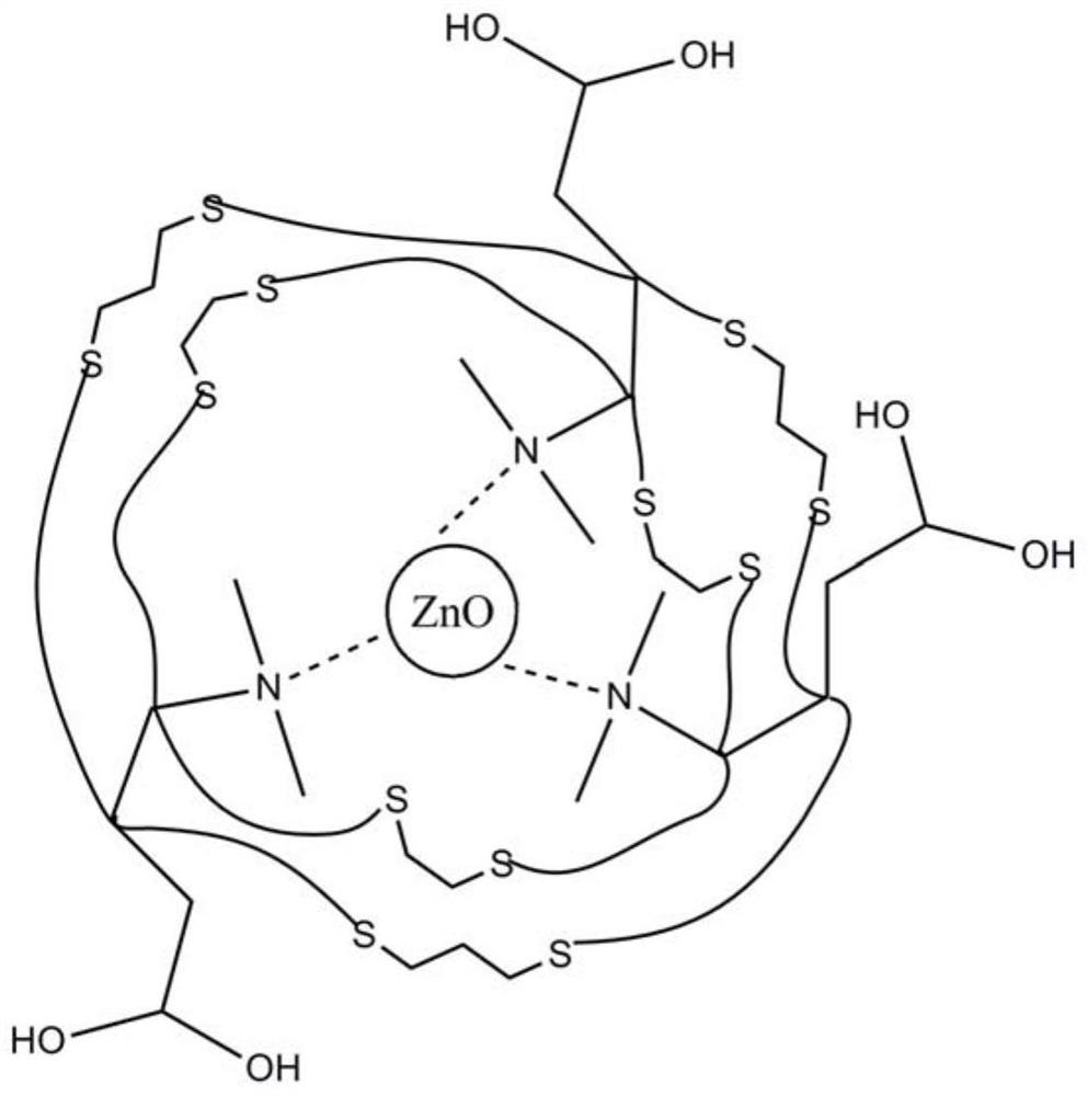
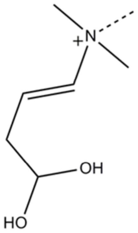
[0034] In this embodiment, the ligand 1 adopts an alcohol amine aliphatic chain with three to eight carbons. By making the zinc oxide nanoparticles 2 adopt the ligand 1 whose chain length is greater than two carbon atoms, compared with the zinc oxide nanoparticles whose ligand is ethanolamine (that is, the ligand chain length is two carbon atoms) in the prior art, increase The steric hindrance between the zinc oxide nanoparticles 2 is avoided, thereby avoiding the aggregation between the zinc oxide nanoparticles 2, and further avoiding the formation of black spots in the film layer formed by using the zinc oxide ink. The crosslinkable group 11 can make self-crosslink...

Embodiment 2

[0053] This embodiment provides an electron transport film layer, which is formed by using the zinc oxide ink in Embodiment 1.

[0054] Wherein, the electron transport film layer can be used as an electron transport layer in an organic electroluminescence device. Zinc oxide ink forms the electron transport film layer by inkjet printing, and its specific preparation method is:

[0055] When the electron transport film layer is formed by printing the zinc oxide ink containing a crosslinkable group in the ligand, the zinc oxide ink is printed on the substrate by inkjet printing, and the substrate loaded with the zinc oxide ink is exposed to ultraviolet light. (Wavelength 365nm) irradiation for about 5 minutes, after the completion of the vacuum degree of 500mbar, heating at 50 degrees for about half an hour to prepare a dense zinc oxide film layer.

[0056] When using zinc oxide ink containing two cross-linkable groups in the ligand to print to form the electron transport film l...

Embodiment 3

[0059] This embodiment provides a display device, including the electron transport film layer in Embodiment 2. The display device is an organic electroluminescence display device.

[0060] By using the electron transport film layer in Example 2, the quality of the display device is improved.

[0061] The display device provided by the present invention can be any product or component with a display function such as an OLED panel, a QLED panel, an OLED TV, a QLED TV, a monitor, a mobile phone, or a navigator.


PUM


Abstract

The invention provides a zinc oxide ink, a preparation method thereof, an electron transport film layer and a display device. The zinc oxide ink comprises zinc oxide nanoparticles loaded with ligands employing aliphatic chains greater than two carbon atoms. The zinc oxide ink adopts a ligand whose chain length is greater than two carbon atoms in the zinc oxide nanoparticle, compared with the zinc oxide nanoparticle whose ligand is ethanolamine (that is, the ligand chain length is two carbon atoms) in the prior art. , increasing the steric hindrance between the zinc oxide nanoparticles, thereby avoiding the aggregation between the zinc oxide nanoparticles, thereby avoiding the formation of black spots in the film layer formed by using the zinc oxide ink; at the same time, the ligand has self-crosslinking properties, form a network structure through self-crosslinking, avoid printing film layers due to too fast solvent volatilization resulting in more holes in the film layer, and ensure the quality of the film layer formed by using the zinc oxide ink.

Description

technical field [0001] The invention relates to the field of display technology, in particular to a zinc oxide ink, a preparation method thereof, an electron transport film layer and a display device. Background technique [0002] Quantum dots (quantum dots, QDs), also known as semiconductor nanocrystals, are nanocrystalline particles with a radius smaller than or close to the radius of a Bohr exciton, and its size is generally between 1-20 nm. Quantum dot light-emitting diode display (quantumdot light emitting device, QLED) is a device that uses colloidal quantum dots as the light-emitting layer and adopts a sandwich structure. QLED has the advantages of high color gamut, self-illumination, low start-up voltage, and fast response, and is currently becoming a very popular research direction. [0003] The electron transport layer in the current QLED usually uses zinc oxide ink and is formed into a film by a printing method (such as an inkjet printing method or a micro-contac...

Claims


Application Information

Patent Timeline
Patent Type & Authority Patents(China)
IPC IPC(8): C09D11/30H01L51/50H01L51/54H10K99/00
CPCC09K11/0811C09D11/52C09D11/36C09D11/322H10K50/16C09D11/037C09D11/033C07F3/06H10K85/381H10K50/115
Inventor 梅文海
Owner BOE TECH GRP CO LTD
Learn More