A graphene-modified au/sno2 structure ammonia sensor and preparation method thereof
An ammonia sensor and graphene technology, applied in the field of sensors, can solve the problems of complex preparation process, poor ammonia response, high working temperature, etc., and achieve the effect of simple process operation, high controllability and low working temperature
- Summary
- Abstract
- Description
- Claims
- Application Information
AI Technical Summary
Problems solved by technology
Method used
Image
Examples
Embodiment 1
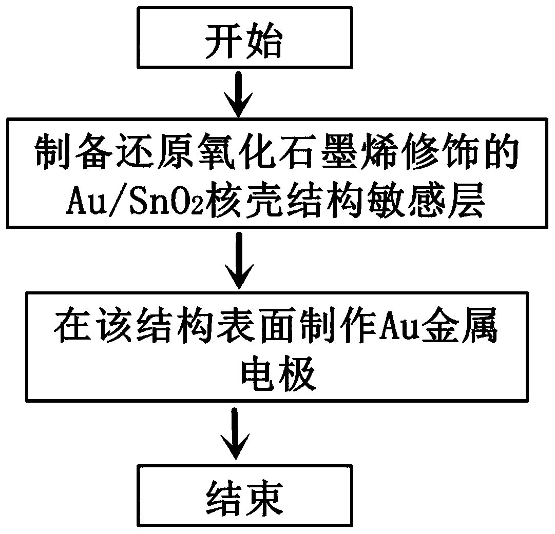
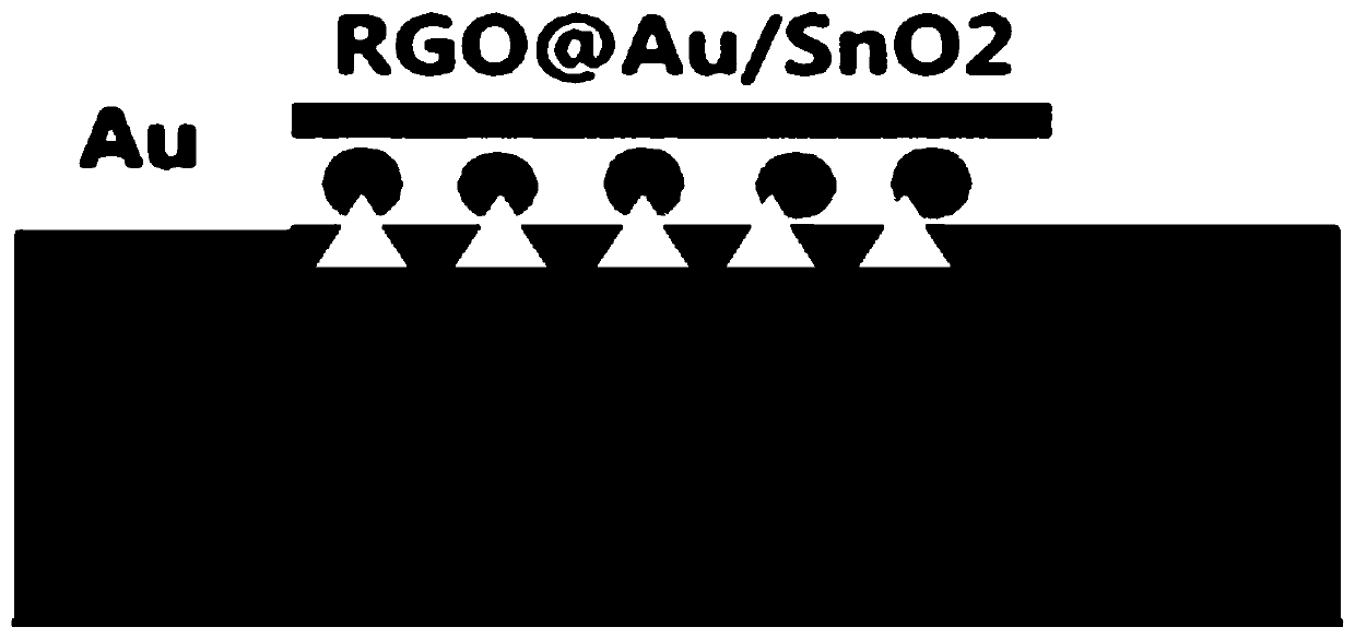
[0065] Step 1), in SiO 2 (500nm) / Si substrate, using magnetron sputtering technology to deposit a gold film with a thickness of about 100nm, and then annealing at a temperature of 900°C for 10min to form Au particles with uniform overall size and controllable distribution. carried out in an argon atmosphere. By controlling the thickness of the gold film, the size of the metal nanoparticles formed after annealing can be effectively controlled to obtain optimal device parameters. If the gold film is too thick to form a continuous film, it is not conducive to the realization of the originally designed core-shell structure, which increases the stability and reliability of the device.
[0066] Step 2), configure HF:NH 4 F is an etching solution with a volume ratio of 1:6, put the sample in step 1) into the etching solution, etch the exposed silicon dioxide layer, the etching depth is 150nm, and clean it with a standard cleaning process after etching. The optimization of annealin...
Embodiment 2
[0074] Step 1), in SiO 2 (500nm) / Si substrate, using magnetron sputtering technology to deposit a gold film with a thickness of about 50nm, and then annealing at a temperature of 950°C for 30min to form Au particles with uniform overall size and controllable distribution. carried out in an argon atmosphere.
[0075] Step 2), configure HF:NH 4 F is an etching solution with a volume ratio of 1:8, put the sample in step 1) into the etching solution, and directional etch the exposed silicon dioxide layer with an etching depth of 100 nm, and clean it with a standard cleaning process after etching.
[0076] Step 3), using magnetron sputtering technology, deposit tin metal on the sample with Au particles distributed in step 2), the deposition time is 30s, forming tin metal covering the entire sample, and then annealing at 800°C for 40min to oxidize the tin Tin dioxide is generated to form a cover of tin dioxide nanoparticles on the gold particles to form a core-shell structure, and...
Embodiment 3
[0082] Step 1), in SiO 2(500nm) / Si substrate, using magnetron sputtering technology to deposit a gold film with a thickness of about 300nm, and then annealing at a temperature of 1000°C for 20min to form Au particles with uniform overall size and controllable distribution. carried out in an argon atmosphere.
[0083] Step 2), configure HF:NH 4 F is an etching solution with a volume ratio of 1:10, put the sample in step 1) into the etching solution, etch the exposed silicon dioxide layer, the etching depth is 300nm, and clean it with a standard cleaning process after etching.
[0084] Step 3), using magnetron sputtering technology, deposit tin metal on the sample with Au particles distributed in step 2), the deposition time is 3 minutes, forming tin metal covering the entire sample, and then annealing at 500 ° C for 60 minutes to oxidize the tin Tin dioxide is generated to form a cover of tin dioxide nanoparticles on the gold particles to form a core-shell structure, and the ...
PUM
| Property | Measurement | Unit |
|---|---|---|
| diameter | aaaaa | aaaaa |
| diameter | aaaaa | aaaaa |
| thickness | aaaaa | aaaaa |
Abstract
Description
Claims
Application Information


