Trench gate charge storage-type IGBT and manufacturing method thereof

A charge storage and charge storage layer technology, applied in semiconductor/solid-state device manufacturing, circuits, electrical components, etc., can solve problems such as oscillation and EMI, and achieve the effects of reducing noise impact, improving switching speed, and reducing gate capacitance

Active Publication Date: 2018-02-23
UNIV OF ELECTRONIC SCI & TECH OF CHINA
View PDF3 Cites 16 Cited by
  • Summary
  • Abstract
  • Description
  • Claims
  • Application Information

AI Technical Summary

Problems solved by technology

[0005] The purpose of the present invention is to reduce the grid-collector capacitance of the device and improve the adverse effects brought by the Miller effect under the condition of certain device trench depth and trench MOS structure density; reduce the overall gate capacitance and improve the device Switching speed, reducing the switching loss of the device, improving the compromise between the forward conduction voltage drop and the turn-off loss of the traditional CSTBT structure; avoiding the current, voltage oscillation

Method used


Image

  • Trench gate charge storage-type IGBT and manufacturing method thereof
  • Trench gate charge storage-type IGBT and manufacturing method thereof
  • Trench gate charge storage-type IGBT and manufacturing method thereof

Examples


Embodiment 1

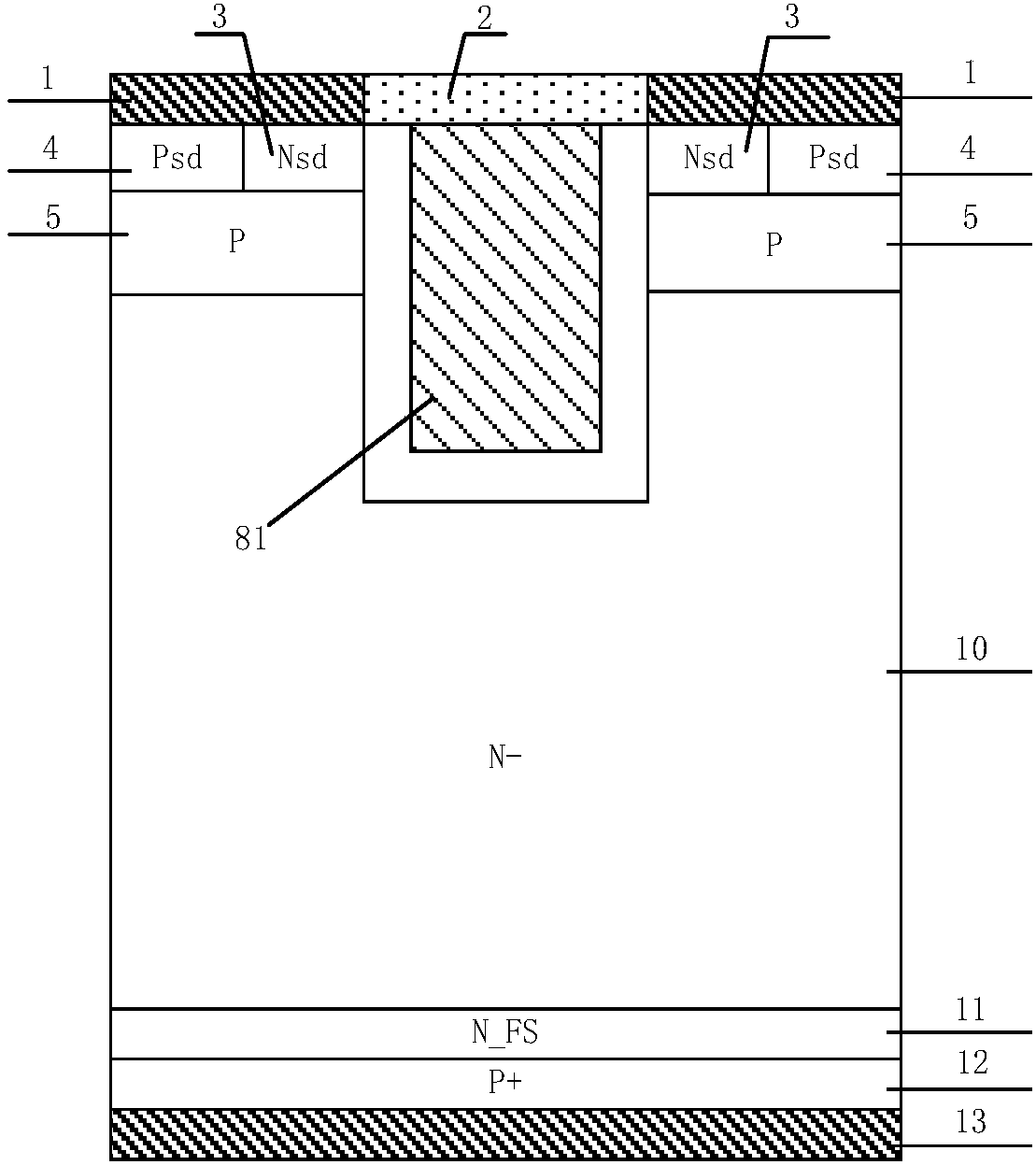
[0085] This embodiment provides a trench gate charge storage type IGBT, the cell structure of which is as follows image 3As shown, the collector metal 13, the P-type collector region 12, the N-type electric field stop layer 11, the N-type drift region 10 and the emitter metal 1 are stacked sequentially from bottom to top; it is characterized in that: the N-type drift The region 10 has an Nsd region 3, a Psd region 4, a P-type base region 5, an N-type charge storage layer 6 and a split trench gate structure; the Nsd region 3 and the Psd region 4 are in contact with each other and are located side by side under the emitter metal 1 and It is connected to the emitter metal 1; the P-type base region 5 is located below the Nsd region 3 and the Psd region 4 and connected to them, and the N-type charge storage layer 6 is located between the P-type base region 5 and the N-type drift region 10; The split trench gate structure includes: gate electrode 81, first gate dielectric layer 82,...

Embodiment 2

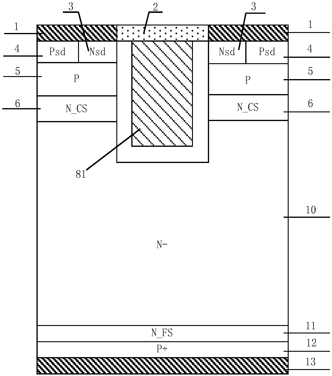
[0087] This embodiment provides a trench gate charge storage type IGBT, the cell structure of which is as follows Figure 4 As shown, the difference from Example 1 is that a part of the lower right corner of the split electrode is etched away to form a ladder-shaped electrode structure, thereby increasing the thickness of the dielectric layer in the lower right corner of the split gate trench structure, thereby obtaining a higher impact breakdown voltage and better reliability.

Embodiment 3

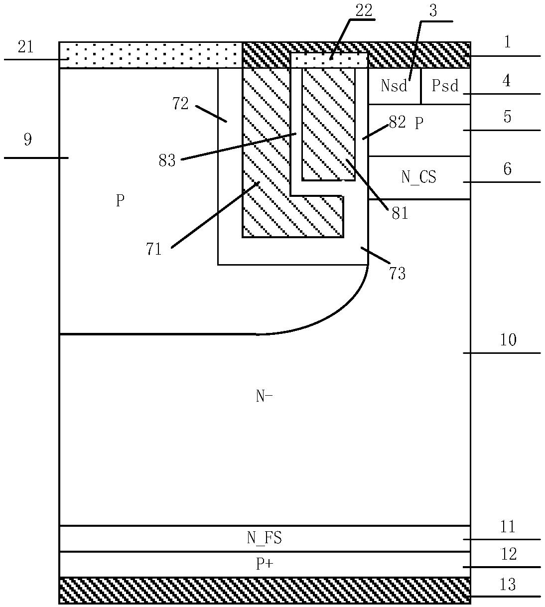
[0089] This embodiment provides a trench gate charge storage type IGBT, the cell structure of which is as follows Figure 5 As shown, the difference from Example 1 is that the split electrodes adopt N-type heavily doped, N-type lightly doped, and P-type doped polysilicon materials sequentially from top to bottom, and the polysilicon is depleted in the blocking state, which will reduce the Collector-emitter capacitance.


PUM

PropertyMeasurementUnit
Thicknessaaaaaaaaaa
Thicknessaaaaaaaaaa

Abstract

The invention discloses a trench gate charge storage-type IGBT and a manufacturing method thereof, which belong to the technical field of power semiconductor devices. Through reasonably introducing asplit trench gate structure and an air floating P-type region, in a condition of not influencing the threshold voltage of the IGBT and conduction, Miller capacitance is reduced, and bad influences brought by Miller effects are improved; the overall gate capacitance is reduced, the device switching speed is improved, the switching losses of the device are reduced, and the compromise between forwardconduction voltage drop and turn-off losses of the traditional CSTBT structure is improved; current and voltage oscillations and EMI problems in the device dynamic starting process are avoided, and the device reliability is improved; electric field concentration effects at the bottom part of the trench are improved, and the breakdown voltage of the device is improved; carrier enhancement effectsat an emitter end of the device are improved, the carrier concentration distribution in a drift region is improved, and the compromise between forward condition voltage drop and turn-off losses is further improved; and besides, the manufacturing method disclosed in the invention has the advantages of low realization difficulty, high product rate and low cost.

Description

technical field [0001] The invention belongs to the technical field of power semiconductor devices, and relates to an insulated gate bipolar transistor (IGBT), in particular to a trench gate charge storage type insulated gate bipolar transistor (CSTBT) and a manufacturing method thereof. Background technique [0002] Insulated Gate Bipolar Transistor (IGBT) is a composite power semiconductor device of MOS Field Effect Transistor (MOSFET) and Bipolar Transistor (BJT). It combines all the advantages of MOS tube and BJT. , the conduction voltage is reduced, and it also has a series of advantages of high voltage resistance, large on-state current, strong current handling capability, and low loss. [0003] Since the IGBT was released in the 1980s, it has attracted the attention of many semiconductor manufacturers and researchers in the world, and has invested a lot of manpower and material resources in the development of IGBT. Now it has become one of the core power semiconductor...

Claims


Application Information

Patent Timeline
IPC IPC(8): H01L29/06H01L29/423H01L29/739H01L21/331H01L21/28
CPCH01L29/0696H01L29/42312H01L29/66348H01L29/7397H01L29/7398
Inventor 张金平田丰境赵倩刘竞秀李泽宏任敏张波
Owner UNIV OF ELECTRONIC SCI & TECH OF CHINA
Why Eureka
Try Eureka