High-performance normally-off GaN field effect transistor and preparation method thereof

A field-effect transistor, normally-off technology, applied in the field of semiconductor device preparation, can solve the problem of reducing the two-dimensional electron gas concentration of the conductive channel in the access area, deteriorating the quality of the secondary epitaxial heterogeneous structure, and detrimental to the conduction performance of the device, etc. problems, to achieve the effect of maintaining high quality, process repeatability and reliability, and improving conduction performance

Pending Publication Date: 2018-02-27
SUN YAT SEN UNIV
View PDF4 Cites 8 Cited by
  • Summary
  • Abstract
  • Description
  • Claims
  • Application Information

AI Technical Summary

Problems solved by technology

The introduction of too many impurities will deteriorate the quality of the secondary epitaxial heterostructure, reduce the two-dimensional electron gas concentration of the conductive channel in the access region, and is not conducive to the improvement of device conduction performance
Therefore, it is necessary to seek a method for optimizing the interface quality of the access region of the normally-off GaN field-effect transistor to overcome the shortcomings of introducing defect impurities into the device access region caused by the selective area growth method, so as to obtain high-performance normally-off GaN field effect transistor

Method used


Image

  • High-performance normally-off GaN field effect transistor and preparation method thereof
  • High-performance normally-off GaN field effect transistor and preparation method thereof
  • High-performance normally-off GaN field effect transistor and preparation method thereof

Examples


Embodiment 1

[0033] Such as Figure 11 Shown is a schematic diagram of the device structure of this embodiment, and its structure includes a substrate 1, a stress buffer layer 2, and a GaN channel layer 3 from bottom to top. Sub-epitaxial layer 4, remove the gate mask to form a groove gate structure and deposit a layer of gate dielectric layer 5 on the surface, remove the gate dielectric layer at both ends of the device to form source 6 and drain 7, and gate dielectric in the groove gate region The layer is covered with a gate 8 .

[0034] The preparation method of the above-mentioned high-performance normally-off GaN field-effect transistor is as follows: Figure 1-Figure 10shown, including the following steps:

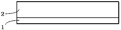
[0035] S1, utilize metal-organic chemical vapor deposition method to grow a layer of stress buffer layer 2 on Si substrate 1, such as figure 1 shown;

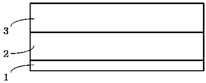
[0036] S2. Using a metal organic chemical vapor deposition method to grow a GaN channel layer 3 on the stress buffer layer ...

Embodiment 2

[0048] Figure 12-14 For the preparation of SiO on the gate region in Example 2 of the present invention 2 Schematic diagram of the process of the mask layer, which is similar to that of SiO on the gate region in Example 1 2 The only difference in the preparation method of the mask layer is that in Example 1, reactive coupled plasma etching is used to form the mask pattern on the gate region, while in Example 2, a lift-off method is used to form the mask pattern on the gate region. film graphics. The specific process includes the following steps:

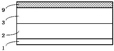
[0049] S1. A photoresist protection layer 10 with a patterned structure is partially formed on the secondary epitaxial layer 3, such as Figure 12 shown;

[0050] S2. Deposit a layer of SiO on the substrate with the photoresist protection layer 10 by plasma enhanced chemical vapor method 2 , as mask layer 9, such as Figure 13 shown;

[0051] S3, using photoresist stripping solution to remove photoresist protective layer 10, ...


PUM


Abstract

The invention relates to the technical field of semiconductor device fabrication, in particular to a high-performance normally-off GaN field effect transistor and a preparation method thereof. The device includes a substrate, an epitaxial layer, a gate dielectric layer, a gate pole, a drain pole and a source pole grown on the substrate. The epitaxial layer includes an epitaxially grown stress buffer layer and a GaN channel layer, masks are only retained in a gate region by mask patterning and etching processes, after mask residues and surface smears in an access region are removed by in-situ etching, an AlGaN/GaN heterojunction structure is grown in a selective region to form a trench channel. A gate metal covers the trench channel, both ends of the transistor form a source region and a drain region, and metals cover the source region and the drain region to form the source pole and the drain pole. The structure of the high-performance normally-off GaN field effect transistor is simple, the preparation process is simple and reliable, the in-situ etching of the access region can reduce defect impurities introduced in the access region of the transistor in a mask preparation process,thereby obtaining a high-quality access region interface and ensuring the secondary epitaxial AlGaN/GaN heterojunction structure quality so as to improve the conduction performance of the normally-off GaN field effect transistor.

Description

technical field [0001] The invention relates to the technical field of semiconductor device preparation, more specifically, to a high-performance normally-off GaN field effect transistor and a preparation method thereof. Specifically, it relates to an improved method for preparing a secondary growth interface of an access region of a recess gate normally-off GaN field effect transistor by selective region epitaxy. Background technique [0002] As a representative of the third-generation semiconductor materials, GaN has the characteristics of large band gap, high critical breakdown electric field strength, high power density and high carrier saturation velocity. GaN power switching devices can greatly increase the upper limit operating frequency while maintaining the low noise performance and high rated power of metal semiconductor field effect transistors, and have the advantages of higher operating voltage, higher power density and high temperature resistance. GaN-based de...

Claims


Application Information

Patent Timeline
Patent Type & Authority Applications(China)
IPC IPC(8): H01L29/778H01L21/335
CPCH01L29/66462H01L29/7786
Inventor 刘扬郑介鑫
Owner SUN YAT SEN UNIV
Why Eureka
Try Eureka