Heterojunction material based on rare earth nickelate-niobium doped strontium titanate and its sensor preparation method and application

A technology of nickelate and strontium titanate, which is applied in the field of sensors, can solve the problems of slow response speed of ultraviolet photodetectors, and achieve the effects of stability, simple structure, and easy epitaxial growth

Active Publication Date: 2019-03-26
HARBIN INST OF TECH
View PDF4 Cites 0 Cited by
  • Summary
  • Abstract
  • Description
  • Claims
  • Application Information

AI Technical Summary

Problems solved by technology

[0004] The present invention is to solve the problem that the response speed of the existing ultraviolet photodetector is relatively slow, and there is no simultaneous self-driven ultraviolet photoelectric sensor and position-sensitive sensor material device, and provides a wide-bandgap semiconductor based heterojunction material and Preparation method and application in self-driven ultraviolet photodetector and position sensitive sensor

Method used


Image

  • Heterojunction material based on rare earth nickelate-niobium doped strontium titanate and its sensor preparation method and application
  • Heterojunction material based on rare earth nickelate-niobium doped strontium titanate and its sensor preparation method and application
  • Heterojunction material based on rare earth nickelate-niobium doped strontium titanate and its sensor preparation method and application

Examples


specific Embodiment approach 1

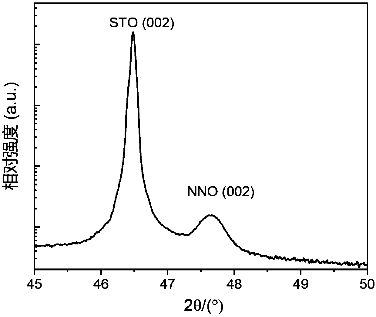
[0027] Specific Embodiment 1: In this embodiment, the heterojunction material based on rare earth nickelate-niobium-doped strontium titanate has a p-n junction structure, and is deposited on an n-type niobium-doped strontium titanate substrate with a thickness of 5~ 20nm p-type nickelate oxide layer, wherein said p-type nickelate oxide is neodymium nickelate (NdNiO 3 ), samarium nickelate (SmNiO 3 ) or gadolinium nickelate (GdNiO 3 ).

specific Embodiment approach 2

[0028] Embodiment 2: This embodiment differs from Embodiment 1 in that the mass concentration of Nb doped in the niobium-doped strontium titanate substrate is 0.05%-0.5%.

specific Embodiment approach 3

[0029] Specific embodiment three: In this embodiment, the sensor preparation method based on the heterojunction material of rare earth nickelate-niobium doped strontium titanate is implemented according to the following steps:

[0030]1. According to the stoichiometric ratio of 1:2, the rare earth oxide and NiO powder are fully mixed, the mixed powder is pressed into tablets, and then sintered at 900-1000°C for pretreatment, and then in a high-purity (99.9995%) oxygen atmosphere at 1100 Sintering at a temperature of ~1400°C to obtain a rare earth nickelate oxide target;

[0031] Second, the Nb:SrTiO 3 The substrate was ultrasonically cleaned in deionized water, acetone and absolute ethanol in sequence for 10-20 minutes to obtain the cleaned Nb:SrTiO 3 Substrate;

[0032] 3. Pump the background vacuum to 2.5~3.5×10 -4 Pa, with cleaned Nb:SrTiO 3 The substrate is used as a deposition substrate, and high-purity oxygen (99.9995%) is introduced to control the air pressure at 0....


PUM

PropertyMeasurementUnit
thicknessaaaaaaaaaa
particle diameteraaaaaaaaaa
band gapaaaaaaaaaa

Abstract

A heterojunction material based on rare earth niobate-niobium doped strontium titanate and a preparation method and an application of a sensor are provided. The invention belongs to the field of sensor, and aims to solve the problem that the existing ultraviolet photoelectric detector responds slowly and is not equipped with both a self-driven ultraviolet photoelectric sensor and a position sensor. The heterojunction material based on rare earth niobate-niobium doped strontium titanate has a p-n junction structure. A p-type nickelate oxide layer with a thickness of 5-20nm is deposited on an n-type niobium doped strontium titanate substrate by laser pulse, wherein the nickelate oxide is neodymium nickelate, samarium nickelate or gadolinium nickelate. The surface of the heterojunction is plated with gold electrodes for preparing a sensor, and the sensor can be applied to self-driven ultraviolet photoelectric detectors and position sensors. Based on the fact that a Nb:SrTiO3 semiconductoronly responds in an ultraviolet / near-ultraviolet light region, the detection range is close to the solar blind area range, and photoelectric response is fast.

Description

technical field [0001] The invention belongs to the field of sensors, and in particular relates to the application of heterojunction longitudinal and lateral photovoltaic effects in self-driven ultraviolet photodetectors and position sensitive sensors. Background technique [0002] Ultraviolet photodetectors have the advantages of high safety, strong anti-interference ability, and no need for human operation. They have very important applications in military and civilian applications such as missile early warning and tracking, ultraviolet communication, environmental monitoring, and biomedical detection. The currently used ultraviolet photodetectors are mainly vacuum photomultiplier tubes, but they have the disadvantages of large volume, fragility, and high power consumption. In practical applications, there are also problems such as low detection sensitivity and photoelectric conversion efficiency. According to the working principle, semiconductor photodetectors are mainly ...

Claims


Application Information

Patent Timeline
Patent Type & Authority Patents(China)
IPC IPC(8): H01L31/109H01L31/032H01L31/18G01D5/26
CPCG01D5/26H01L31/032H01L31/109H01L31/18Y02P70/50
Inventor 王先杰周倩胡昌隋郁宋波
Owner HARBIN INST OF TECH
Why Eureka
Try Eureka