Cu2O/GaOOH nano core-shell pn junction photoelectric detector and preparation method thereof

A technology of photodetectors and nano-core shells, applied in the field of photodetectors, can solve the problems of relatively high pH requirements, poor repeatability, and high cost, and achieve the effects of uniform distribution, low cost, and high utilization efficiency

Active Publication Date: 2018-03-20
ZHEJIANG SCI-TECH UNIV
View PDF4 Cites 9 Cited by
  • Summary
  • Abstract
  • Description
  • Claims
  • Application Information

AI Technical Summary

Problems solved by technology

Among them, the magnetron sputtering method requires a certain vacuum condition, and the method is complicated to operate and expensive; the electrochemic

Method used


Image

  • Cu2O/GaOOH nano core-shell pn junction photoelectric detector and preparation method thereof
  • Cu2O/GaOOH nano core-shell pn junction photoelectric detector and preparation method thereof
  • Cu2O/GaOOH nano core-shell pn junction photoelectric detector and preparation method thereof

Examples


Embodiment 1

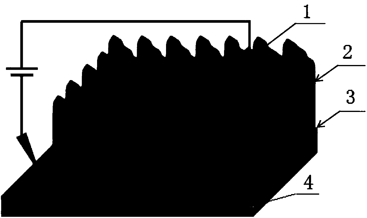
[0034] a Cu 2 Preparation method of O / GaOOH nano core-shell pn junction photodetector, coating a layer of Ga on FTO conductive glass 2 o 3 seed layer, using a hydrothermal method on Ga 2 o 3 GaOOH nanocolumn arrays are grown on the seed layer, and copper salt solution is added to the water bath to grow Cu 2 O nanocrystals, forming Cu 2 O / GaOOH nano-core-shell nanoarrays. Also included in Cu 2 O / GaOOH nano-core-shell nano-array coated with silver electrodes.

[0035] Cu 2 The specific steps of the preparation method of the O / GaOOH nano core-shell pn junction photodetector are as follows:

[0036] (1) Pretreatment of FTO conductive glass substrate: ultrasonic cleaning with acetone, absolute ethanol, and deionized water for 10 minutes, and then drying in an oven;

[0037] (2) Preparation of the seed layer solution: Take 18 μL of ethanolamine, 0.0741 g of gallium isopropoxide, and 2.98 mL of ethylene glycol methyl ether into a 5 mL beaker, heat in a water bath at 60 °C fo...

Embodiment 2

[0044] The difference between this embodiment and embodiment 1 is that the Ga(NO 3 ) 3 The concentration of the growth solution was 0.3g / 30mL, and the growth time was 12 hours at 150°C in a stainless steel autoclave, and the rest were the same as in Example 1.

[0045] Specifically, Cu 2 The specific steps of the preparation method of the O / GaOOH nano core-shell pn junction photodetector are as follows:

[0046] (1) Pretreatment of FTO conductive glass substrate: ultrasonic cleaning with acetone, absolute ethanol, and deionized water for 10 minutes, and then drying in an oven;

[0047] (2) Preparation of the seed layer solution: Take 18 μL of ethanolamine, 0.0741 g of gallium isopropoxide, and 2.98 mL of ethylene glycol methyl ether into a 5 mL beaker, heat in a water bath at 60 °C for 60 min, cool and place in a refrigerator for later use ;

[0048] (3) Preparation of the seed crystal layer: the FTO conductive glass substrate after step 1) is fixed on the glue homogenizin...

Embodiment 3

[0054] The difference between this example and Example 1 is that the amount of 80% hydrazine hydrate solution added in step (6) is 300 μL, and the rest are the same as Example 1.

[0055] Specifically, Cu 2 The specific steps of the preparation method of the O / GaOOH nano-core-shell pn junction photodetector are as follows: (1) Pretreatment of the FTO conductive glass substrate: ultrasonic cleaning with acetone, absolute ethanol, and deionized water for 10 min, and then drying in an oven ;

[0056] (2) Preparation of the seed layer solution: Take 18 μL of ethanolamine, 0.0741 g of gallium isopropoxide, and 2.98 mL of ethylene glycol methyl ether into a 5 mL beaker, heat in a water bath at 60 °C for 60 min, cool and place in a refrigerator for later use ;

[0057] (3) Preparation of the seed crystal layer: the FTO conductive glass substrate after step 1) is fixed on the glue homogenizing sample stage of the rubber homogenizing / glue drying machine, drips a certain amount of 0.1...


PUM

PropertyMeasurementUnit
Thicknessaaaaaaaaaa

Abstract

The invention belongs to the field of photoelectric detectors, and specifically relates to a Cu2O/GaOOH nano core-shell pn junction photoelectric detector and a preparation method thereof. The Cu2O/GaOOH nano core-shell pn junction photoelectric detector comprises an Ag electrode, Cu2O nano-crystals, a GaOOH nano-column array, a Ga2O3 seed crystal layer and FTO conductive glass, and is characterized in that the Ga2O3 seed crystal layer is located on the FTO conductive glass, the Cu2O/GaOOH nano-column array is located on the Ga2O3 seed crystal layer, Cu2O/GaOOH nano-columns are formed by GaOOHnano-columns and the Cu2O nano-crystals, the GaOOH nano-column array is located on the Ga2O3 seed crystal layer, and the Cu2O nano-crystals wrap the outer periphery of the GaOOH nano-columns. The Cu2O/GaOOH nano core-shell pn junction prepared according to the invention has a large specific surface area, is strong in absorption for light, can achieve wide-spectrum detection and provides an effective method for constructing a high-performance photoelectric detector. The preparation method is simple to operate, low in cost and good in repeatability, and certainly has great application prospectsin the photoelectric field in the future.

Description

technical field [0001] The invention belongs to the field of photodetectors, in particular to a Cu 2 O / GaOOH nano core-shell pn junction photodetector and its preparation method. technical background [0002] Semiconductor devices have been widely used in medical and health care, scientific research and teaching, and national defense technology. However, how to improve the optical, electrical, and thermal properties of semiconductor materials and improve their controllability has gradually become a research hotspot. The heterojunction is the interface region formed by the contact of two different semiconductors. By forming a built-in electric field, the electron-hole pairs can be effectively separated and the recombination can be reduced. Therefore, it has excellent photoelectric characteristics that cannot be achieved by the two semiconductors, and in It has broad application prospects in the fields of making ultra-high-speed switching devices, solar cells, semiconductor l...

Claims


Application Information

Patent Timeline
IPC IPC(8): H01L51/46H01L51/42H01L51/48B82Y30/00B82Y40/00
CPCB82Y30/00B82Y40/00H10K71/15H10K85/00H10K30/15Y02E10/549
Inventor 赵海林李小云陈凯樊寅翔陈露魏亚菊王顺利郭道友李培刚
Owner ZHEJIANG SCI-TECH UNIV
Why Eureka
Try Eureka