

Silicon carbide MOSFET and manufacture method thereof
A technology of silicon carbide and oxide, which is applied in the field of microelectronics, can solve the problems of high interface density of silicon carbide MOSFETs, achieve the effects of reducing dangling bonds, small threshold voltage shift, and easing interface stress
- Summary
- Abstract
- Description
- Claims
- Application Information
AI Technical Summary
Problems solved by technology
Method used
Image

Examples
no. 1 example
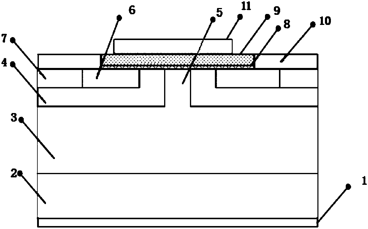
[0029] This embodiment provides a silicon carbide MOSFET, figure 1 is a schematic diagram of the MOSFET, as figure 1 As shown, the MOSFET includes the following components from bottom to top: drain metal 1, N + Substrate 2, N - Drift layer 3, P well 4, JFET region 5, N+ source region 6, P+ contact region 7, group II alkaline earth metal oxide interface layer 8, SiO 2 Gate dielectric layer 9 , source metal 10 and polysilicon 11 .
[0030] like figure 1 As shown, the interface layer formed by the alkaline earth metal oxide is vertically arranged on the SiO of the MOSFET 2 Between the gate dielectric layer and the JFET region, two N + between source contacts.
[0031] The alkaline earth metal oxides involved in this embodiment are group II alkaline earth metal oxides, and the thickness of the interface layer formed by the alkaline earth metal oxides can be 0.3 to 5 nm, wherein SiO 2 The thickness of the gate dielectric layer is 30nm-150nm, wherein the alkaline earth metal ...
no. 2 example
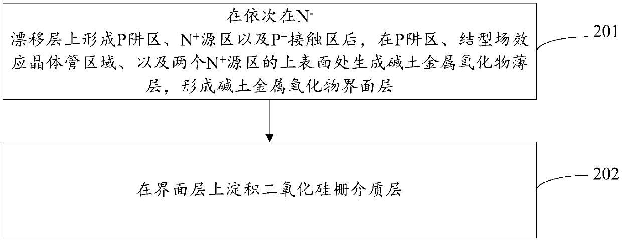
[0036] This embodiment provides a silicon carbide MOSFET manufacturing method, which is used to manufacture the silicon carbide MOSFET provided in the first embodiment above, figure 2 is the flowchart of the method, such as figure 2 As shown, the method includes the following steps:
[0037] Step 201: in sequence in N - P well region, N + source region and P + After the contact area, in the P well area, the junction field effect transistor JFET area, and the two N + A thin layer of alkaline earth metal oxide is formed on the upper surface of the source region to form an alkaline earth metal oxide interface layer;
[0038] Optionally, the alkaline earth metal oxides involved in this embodiment are group II alkaline earth metal oxides.
[0039] Step 202: Deposit SiO on the interface layer 2 gate dielectric layer.
[0040] Among them, the alkaline earth metal oxide interfacial layer is vertically arranged on SiO 2 Between the gate dielectric layer and the JFET region, i...
no. 3 example
[0046] In this embodiment, on the basis of the above-mentioned embodiment 2, the whole process of making silicon carbide MOSFET is described in detail, as Figures 3 to 10 As shown, the preparation method provided in this embodiment includes the following steps:
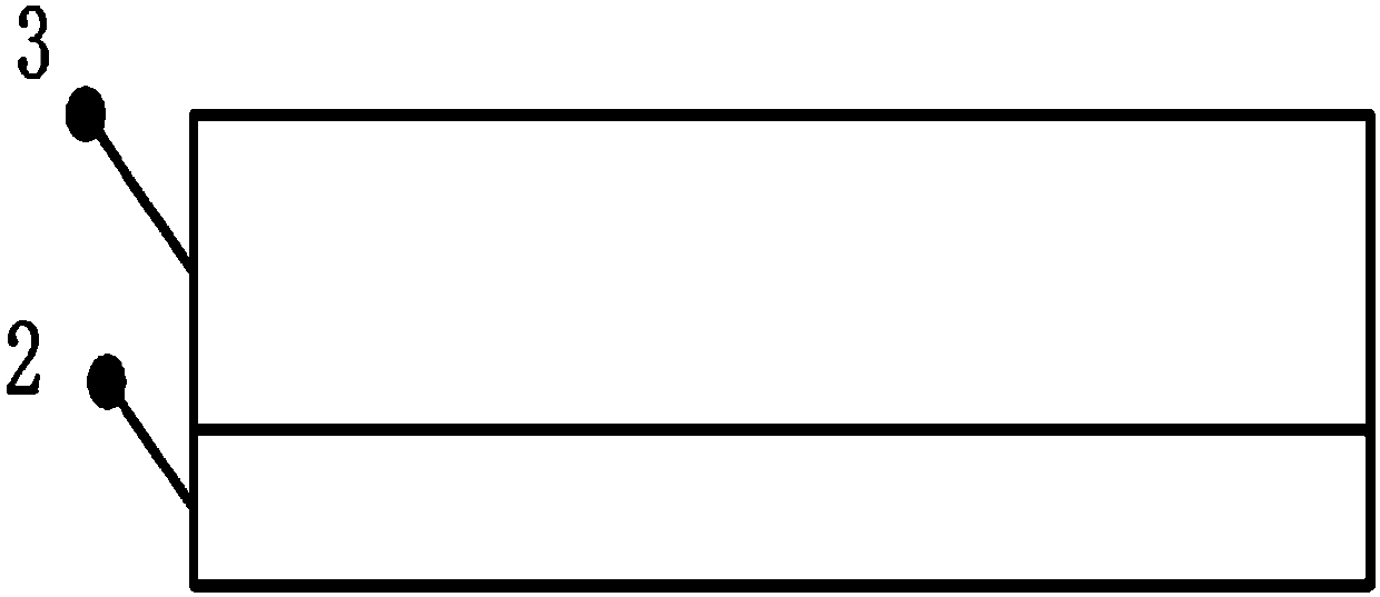
[0047] Step 1: In N + Epitaxial growth of N on SiC substrate 2 - Drift layer 3, such as image 3 shown.
[0048] to N + The silicon carbide substrate was cleaned by RCA cleaning standard, and then epitaxially grown on the surface of the substrate with a thickness of 8 μm and a nitrogen ion doping concentration of 1×10 15 cm -3 N - The process conditions for the drift layer are: the epitaxy temperature is 1570°C, the pressure is 100mbar, the reaction gas is silane and propane, the carrier gas is pure hydrogen, and the impurity source is liquid nitrogen.
[0049] Step 2: In N - Multiple times of selective implantation of aluminum ions is performed on the drift layer 3 to form a P well region 4, such as Figure...
PUM
| Property | Measurement | Unit |
|---|---|---|
| Thickness | aaaaa | aaaaa |
| Thickness | aaaaa | aaaaa |
| Thickness | aaaaa | aaaaa |
Abstract
Description
Claims
Application Information