

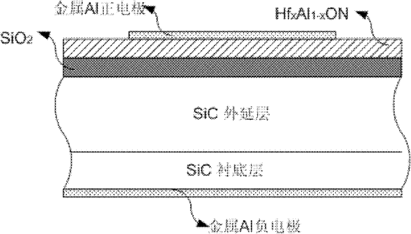
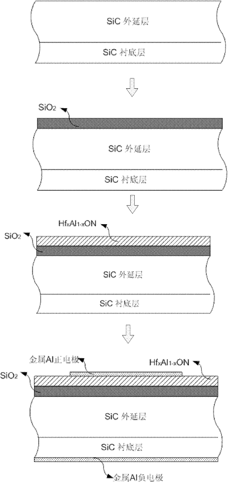
Silicon carbide (SiC) metal oxide semiconductor (MOS) capacitor with composite dielectric layer and manufacturing method for SiC MOS capacitor with composite dielectric layer
A composite medium and manufacturing method technology, applied in the field of microelectronics, can solve the problems of not improving the reliability of the oxide layer, reducing the interface state density of the device, and the lattice damage of the oxide layer interface, so as to increase the maximum critical electric field and reduce the interface state density , Improve the effect of pressure resistance
- Summary
- Abstract
- Description
- Claims
- Application Information
AI Technical Summary
Problems solved by technology
Method used
Image

Examples
Embodiment 1
[0031] Step 1, growing an N-type SiC epitaxial layer.
[0032] The thickness is 380μm, the doping concentration is 5×10 18 cm -3 The N-type SiC substrate material is placed in a SiC epitaxial growth furnace, the growth temperature is 1570 °C, the thickness of the growth layer is 10 μm, and the doping concentration is 5×10 15 cm - 3 N-type SiC epitaxial wafers.
[0033] In step 2, pretreatment is performed on the grown N-type SiC epitaxial wafer.
[0034] 2.1) Ultrasonic cleaning of the N-type SiC epitaxial wafer with deionized water;
[0035] 2.2) Clean the SiC epitaxial wafer with 80% sulfuric acid, boil for 10 minutes, then soak for 30 minutes;
[0036] 2.3) Clean the SiC epitaxial wafer several times with deionized water;
[0037] 2.4) Use H at a ratio of 5:1:1 2 O, H 2 o 2 and hydrochloric acid, soak the SiC epitaxial wafer in the mixed solution at a temperature of 80°C for 5 minutes, wash it with hydrofluoric acid solution, and then wash it several times with deion...
Embodiment 2
[0051] Step 1, growing an N-type SiC epitaxial layer.
[0052] The thickness is 380μm, the doping concentration is 5×10 18 cm -3 The N-type SiC substrate material is placed in a SiC epitaxial growth furnace, the growth temperature is 1570 °C, the thickness of the growth layer is 50 μm, and the doping concentration is 2×10 15 cm -3 N-type SiC epitaxial wafer.
[0053] In step 2, pretreatment is performed on the grown N-type SiC epitaxial wafer.
[0054] First, ultrasonically clean the N-type SiC epitaxial wafer with deionized water;
[0055] Next, clean the SiC epitaxial wafer with 80% sulfuric acid, boil for 10 minutes, and soak for 30 minutes;
[0056] Next, wash the SiC epitaxial wafer several times with deionized water;
[0057] Then, with H at a ratio of 5:1:1 2 O, H 2 o 2 and hydrochloric acid, soak the SiC epitaxial wafer in the mixed solution at a temperature of 80° C. for 5 minutes, wash it with hydrofluoric acid solution, wash it several times with deionized ...
Embodiment 3
[0071] Step A, growing an N-type SiC epitaxial layer.
[0072] The thickness is 380μm and the doping concentration is 5×10 18 cm -3 The N-type SiC substrate was placed in a SiC epitaxial furnace for growth at a growth temperature of 1600 °C, a layer thickness of 100 μm, and a doping concentration of 1×10 15 cm -3 N-type SiC epitaxial layer.
[0073] Step B, performing pretreatment on the grown N-type SiC epitaxial wafer.
[0074] B1) Ultrasonic cleaning of the N-type SiC epitaxial wafer with deionized water;
[0075] B2) Clean the SiC epitaxial wafer with 80% sulfuric acid, boil it for 10 minutes, then soak it for 30 minutes;
[0076] B3) Clean the SiC epitaxial wafer several times with deionized water;
[0077] B4) H in a ratio of 5:1:1 2 O, H 2 o 2 and hydrochloric acid, soak the SiC epitaxial wafer in the mixed solution at a temperature of 80° C. for 5 minutes, wash it with hydrofluoric acid solution, wash it several times with deionized water, and finally dry it w...
PUM
| Property | Measurement | Unit |
|---|---|---|
| Thickness | aaaaa | aaaaa |
| Doping concentration | aaaaa | aaaaa |
| Thickness | aaaaa | aaaaa |
Abstract
Description
Claims
Application Information