

Method for manufacturing low-offset flat band voltage SiC MOS capacitor
A manufacturing method and flat-band voltage technology, applied in the field of microelectronics, can solve problems such as difficult nitrogen-containing gas dosage, influence on device interface characteristics, large flat-band voltage offset, etc., to reduce dangling bonds, reduce near-interface trap density, The effect of small flat-band voltage excursions
- Summary
- Abstract
- Description
- Claims
- Application Information
AI Technical Summary
Problems solved by technology
Method used
Image

Examples
Embodiment 1
[0020] Embodiment 1, comprises the steps:
[0021] Step 1, first clean the N-SiC epitaxial material with deionized water ultrasonically, then clean it with concentrated sulfuric acid, heat it to smoke, boil for 10 minutes, soak for 30 minutes, and rinse the surface with deionized water several times; then use a ratio of 5 : 1:1 H 2 O, H 2 o 2 The No. 1 mixed liquid composed of ammonia water was soaked in a water bath for N-SiC epitaxial materials at a temperature of 80°C for 5 minutes, and after being washed with hydrogen fluoride solution, the surface was rinsed several times with ionized water; 2 O, H 2 o 2 The No. 2 mixed liquid composed of HCl was soaked in a water bath for 5 minutes at a temperature of 80 ° C, and the N-SiC epitaxial material was washed with a hydrogen fluoride solution, and the surface was rinsed several times with ionized water; finally, it was dried with an infrared lamp.
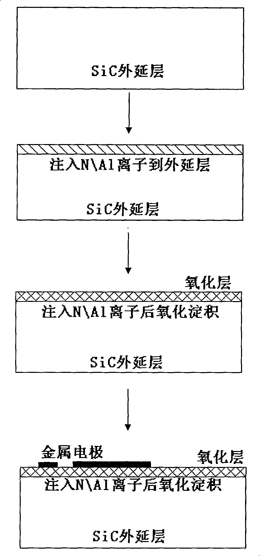
[0022] Step 2, perform N on the epitaxial layer after cleaning + Ion impl...
Embodiment 2
[0027] Embodiment 2, comprises the steps:
[0028] Step 1, first clean the N-SiC epitaxial material with deionized water ultrasonic cleaning, then clean it with concentrated sulfuric acid, and heat it to smoke, boil for 10 minutes, soak for 30 minutes, and rinse the surface with deionized water several times; then use a ratio of 5:1:1 H 2 O, H 2 o 2 The No. 1 mixed liquid composed of ammonia water was soaked in a water bath for N-SiC epitaxial materials at a temperature of 80°C for 5 minutes, and after being washed with hydrogen fluoride solution, the surface was rinsed several times with ionized water; 2 O, H 2 o 2 The No. 2 mixed liquid composed of HCl was soaked in a water bath for 5 minutes at a temperature of 80 ° C, and the N-SiC epitaxial material was washed with a hydrogen fluoride solution, and the surface was rinsed several times with ionized water; finally, it was dried by an infrared lamp.
[0029] Step 2, perform N on the epitaxial layer after cleaning + Ion...
Embodiment 3
[0034] Embodiment 3, comprises the steps:
[0035] Step 1, first clean the N-SiC epitaxial material with deionized water ultrasonically, then clean it with concentrated sulfuric acid, heat it to smoke, boil for 10 minutes, soak for 30 minutes, and rinse the surface with deionized water several times; then use a ratio of 5 : 1:1 H 2 O, H 2 o 2 The No. 1 mixed liquid composed of ammonia water was soaked in a water bath for N-SiC epitaxial materials at a temperature of 80°C for 5 minutes, and after being washed with hydrogen fluoride solution, the surface was rinsed several times with ionized water; 2 O, H 2 o 2 The No. 2 mixed liquid composed of HCl was soaked in a water bath for 5 minutes at a temperature of 80 ° C, and the N-SiC epitaxial material was washed with a hydrogen fluoride solution, and the surface was rinsed several times with ionized water; finally, it was dried by an infrared lamp.
[0036] Step 2, perform N on the epitaxial layer after cleaning + Ion implan...
PUM
| Property | Measurement | Unit |
|---|---|---|
| Thickness | aaaaa | aaaaa |
| Thickness | aaaaa | aaaaa |
| Diameter | aaaaa | aaaaa |
Abstract
Description
Claims
Application Information