Method for improving charge accumulation in GaN HEMT (High Electron Mobility Transistor) surface electron beam direct writing

A technology of charge accumulation and electron beam, applied in the direction of circuits, electrical components, semiconductor devices, etc., to achieve good adhesion, improve charge accumulation, and good electrical conductivity

Active Publication Date: 2018-04-13
NO 55 INST CHINA ELECTRONIC SCI & TECHNOLOGYGROUP CO LTD
View PDF6 Cites 9 Cited by
  • Summary
  • Abstract
  • Description
  • Claims
  • Application Information

AI Technical Summary

Problems solved by technology

[0006] The present invention proposes a method for solving electron beam charge accumulation on the surface of GaN HEMT, the purpose of which is to solve the problem of charge accumulation in the process of electron beam direct writing, and at the same time effectively solve the problems of direct writing overlay and adhesion

Method used


Image

  • Method for improving charge accumulation in GaN HEMT (High Electron Mobility Transistor) surface electron beam direct writing
  • Method for improving charge accumulation in GaN HEMT (High Electron Mobility Transistor) surface electron beam direct writing
  • Method for improving charge accumulation in GaN HEMT (High Electron Mobility Transistor) surface electron beam direct writing

Examples


preparation example Construction

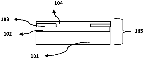
[0028] (1) Preparation of components: On the GaN HEMT epitaxial material, use photolithography to obtain source and drain patterns; prepare source and drain metal systems by electron beam evaporation, stripping and alloying; use enhanced plasma chemical vapor deposition or coupled inductance chemistry A layer of protective dielectric SiN is prepared by vapor deposition method, and the thickness of the SiN is 40nm~200nm; the resistance metal and the capacitor bottom electrode metal are sequentially prepared by ultraviolet lithography, evaporation and sputtering processes;

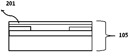
[0029] (2) Preparation of nano-thin metal germanium: nano-thin metal germanium is prepared by electron beam evaporation process or sputtering process, with a thickness of 0~10nm;

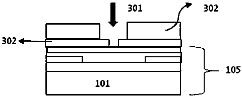
[0030] (3) Electron beam direct writing grid: the preparation of the grid adopts the electron beam direct writing process. The prepared grid is a T-shaped grid or a Y-shaped grid. The grid metal is coated with no less than 2 layers...

Embodiment 1

[0042] A method for improving the charge accumulation of GaN HEMT surface electron beam direct writing, comprising the following steps:

[0043] 1) On the HEMT epitaxial material of the GaN substrate, the source-drain pattern is obtained by photolithography, and then the source-drain metal system is prepared by electron beam evaporation, stripping and alloying, and then a layer of protective dielectric SiN is grown. SiN can be enhanced Prepared by plasma chemical vapor deposition, the thickness is 40nm. Then, resistive metal and capacitor lower electrode metal are sequentially prepared by ultraviolet lithography, evaporation or sputtering and other processes;

[0044] 2) A layer of 5nm-thick metal germanium was prepared by electron beam evaporation process. Then apply electron beam glue, bake, and direct write. Among them, the preparation of GaN small gate length adopts the method of electron beam one-time forming, which needs to apply multiple layers of glue and direct write...

Embodiment 2

[0050] 1) On the HEMT epitaxial material of the GaN substrate, the source-drain pattern is obtained by photolithography, and then the source-drain metal system is prepared by electron beam evaporation, stripping and alloying processes, and then a layer of protective dielectric SiN is grown. SiN can use coupled inductors Prepared by chemical vapor deposition method, the thickness is 200nm. Then, resistive metal and capacitor lower electrode metal are sequentially prepared by ultraviolet lithography, evaporation or sputtering and other processes;

[0051] 2) Prepare a layer of 10nm-thick metal germanium by electron beam sputtering process. Then apply electron beam glue, bake, and direct write. The preparation of GaN small gate length generally adopts the method of electron beam one-time forming, which needs to apply multiple layers of glue and direct write multiple times. Both have the function of eliminating charge accumulation;

[0052] 3) The developed sample is corroded an...


PUM


Abstract

The invention relates to a method for improving charge accumulation in GaN HEMT (High Electron Mobility Transistor) surface electron beam direct writing. The method is characterized by comprising theprocessing steps of (1) preparation of components; (2) preparation of nanometer thin layer metal germanium; (3) preparation of an electron beam direct writing gate; (4) first removing of the nanometerthin layer metal germanium; (5) etching of a gate dielectric, and evaporation and stripping of gate metal; and (6) second removing of the nanometer thin layer metal germanium. The advantages are that1, the metal germanium is adopted to serve as a bottom conductive layer, the consistency is good, the thickness can be accurately controlled, and an electron beam adhesive coated at the surface has good adhesion and is easy to be removed; 2, the metal germanium with the thickness being below 10nm can have very good conductive characteristics and has an excellent effect for improving charge accumulation of GaN HEMT surface electron beams.

Description

technical field [0001] The invention relates to a method for improving charge accumulation of GaN HEMT surface electron beam direct writing, which belongs to the technical field of semiconductor device and integrated circuit manufacturing technology. Background technique [0002] In the manufacturing process of modern semiconductor devices, with the advancement of technology, the device size is getting smaller and smaller, and the integration level is getting higher and higher. The third-generation semiconductor GaN has broad application prospects in the high-frequency field of microwave and millimeter-wave chips. Millimeter-wave GaNHEMT devices have the advantages of high operating voltage, output power up to watt level, high power density, and operating frequency up to 100GHz. GaN HEMT devices, especially AlGaN / GaN HEMT structures, have poor surface conductivity. Moreover, it is generally necessary to grow a dense layer of SiN dielectric on the surface before making the ...

Claims


Application Information

Patent Timeline
Patent Type & Authority Applications(China)
IPC IPC(8): H01L29/778H01L21/335H01L29/423H01L21/28
CPCH01L21/28026H01L29/42372H01L29/66431H01L29/7783
Inventor 吴少兵高建峰
Owner NO 55 INST CHINA ELECTRONIC SCI & TECHNOLOGYGROUP CO LTD
Why Eureka
Try Eureka