Semiconductor photoelectrode photocatalytic water splitting reaction device based on black silicon PN knots and manufacturing method thereof

A reaction device, PN junction technology, applied in the direction of electrodes, electrolysis process, electrolysis components, etc., can solve the problem of low light utilization rate of ordinary silicon wafers, achieve the effect of improving the efficiency of photolysis of water, reducing costs, and simple principle

Inactive Publication Date: 2018-05-08
CHINA UNIV OF MINING & TECH
View PDF9 Cites 1 Cited by
  • Summary
  • Abstract
  • Description
  • Claims
  • Application Information

AI Technical Summary

Problems solved by technology

[0006] The purpose of the present invention is to provide a semiconductor photoelectrode photo-water splitting reaction device and preparation method based on black silicon PN junction, so as to solve the problem of low light utilization rate of ordinary silicon wafers

Method used


Image

  • Semiconductor photoelectrode photocatalytic water splitting reaction device based on black silicon PN knots and manufacturing method thereof
  • Semiconductor photoelectrode photocatalytic water splitting reaction device based on black silicon PN knots and manufacturing method thereof
  • Semiconductor photoelectrode photocatalytic water splitting reaction device based on black silicon PN knots and manufacturing method thereof

Examples


preparation example Construction

[0033] The preparation method of the black silicon PN junction photoelectrode is as follows:

[0034] (1) After micronizing the surface of ordinary P-type single crystal or polycrystalline silicon wafers to form black silicon, after low-temperature and low-concentration source diffusion process, the obtained black silicon wafers are preheated in a diffusion furnace at 750-800°C and passed through into low concentration O 2 , the flow rate is 0.1-0.2L / min, and the surface of the black silicon wafer is slightly oxidized in advance;

[0035] (2) Then feed POCl3 with a flow rate of 0.9-1.5L / min, and form a uniform black silicon PN junction after phosphorus diffusion at 800-870°C for 30-60 minutes;

[0036] (3) Finally, use hydrofluoric acid to remove the phosphosilicate glass layer on the surface of the PN junction black silicon.

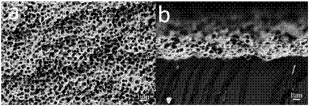
[0037] The surface micronanoization is a structure combining micro pits and nano pits, and the size of the nano pits is 10-900nm, and the depth is 10...

Embodiment 1

[0042] 1. Take a P-type polycrystalline silicon wafer, and prepare a polycrystalline black silicon wafer with a micro-nano structure by using Ag as a metal catalyst through the MACE method.

[0043] 2. Using phosphorus oxychloride (POCl 3 ) Liquid source diffusion process to prepare PN junction:

[0044] a) Place the textured black silicon wafer on a quartz boat, push it into the furnace chamber, and then raise the temperature to 800°C and feed nitrogen gas at a flow rate of 15L / min, and keep it warm for 15 minutes for preheating.

[0045] b) Pass O 2 , the flow rate is 0.1L / min, and the temperature is kept for 1.5min to pre-oxidize the micro-nano structure on the surface of the black silicon.

[0046] c) Introduce nitrogen with a flow rate of 5 L / min and keep warm for 5 minutes to pre-deposit micro-nano structures on the surface of the black silicon.

[0047] d) Raise the temperature to 810°C, feed in nitrogen and oxygen, keep it warm for 10 minutes, and carry out back-tempe...

Embodiment 2

[0059] 1. Take a P-type polycrystalline silicon wafer, and prepare a polycrystalline black silicon wafer with a micro-nano structure by using Ag as a metal catalyst through the MACE method.

[0060] 2. Adopt the same diffusion process steps as in Example 1, but change the step g) temperature to 870°C, and the process time is 18min, and other process parameters are the same as in Example 1 to prepare PN junction black silicon, which is measured by the four-probe method The average square resistance of the black silicon wafer is 103Ω / □.

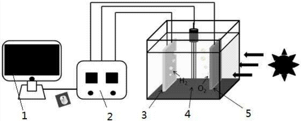
[0061] 3. Assembling and constructing the photo-water splitting reaction device of black silicon PN junction: polycrystalline PN junction black silicon with a square resistance of 103Ω / □ is used as the photoelectrode, the saturated Ag / AgCl electrode is used as the reference electrode, and the Pt electrode is used as the counter electrode. The 0.2mol / L Na2SO4 solution was used as the electrolyte, and the photoelectric water splitting reaction de...


PUM

PropertyMeasurementUnit
depthaaaaaaaaaa

Abstract

The invention discloses a semiconductor photoelectrode photocatalytic water splitting device based on black silicon PN knots and a manufacturing method thereof, and belongs to a semiconductor photoelectrode manufacturing method and a photocatalytic water splitting reaction device. (1), after the surface of an ordinary P-type monocrystal or polycrystalline silicon wafer is micro-nanocrystallized toform black silicon, the obtained black silicon wafer is placed into a diffusion furnace to be preheated at 750-800 DEG C through a low-temperature low-density source diffusion technique, and O2 withthe flow of 0.1-0.2 L / min is introduced in, so that the surface of the black silicon wafer is slightly oxidized; then POCl3 with the flow of 0.9-1.5 L / min is introduced in, and diffusion is performedfor 30-80 min at 800-870 DEG C, so that uniform black silicon PN knots are formed; finally, phosphorosilicate glass layers on the surfaces of the black silicon PN knots are removed by using hydrofluoric acid. The semiconductor photoelectrode photocatalytic water splitting device has the advantages that solar energy is utilized for driving, so that only a little external force driving is needed; the principle is simple; assembly is easy; cost is low; the reflectivity of the silicon wafer is lowered to 2%-15%, so that utilization of light is improved; and the uniform PN knots are manufactured through the diffusion technique, so that photocatalytic water splitting efficiency of the device is further improved.

Description

technical field [0001] The invention relates to a semiconductor photoelectrode preparation method and a photolysis water reaction device, and is characterized in that a semiconductor photoelectrode photolysis water reaction device and a preparation method based on a black silicon PN junction. Background technique [0002] With the increasing depletion of earth's energy, traditional fossil energy will eventually be exhausted, and the pollution caused by traditional fossil energy has seriously affected the living environment of human beings. In order to solve the energy crisis and continuously improve the living environment of human beings, the development of new clean energy is imminent. Among them, hydrogen production by photolysis of water is a clean and efficient way, so it has become the focus of new energy research. [0003] By constructing an electrochemical cell, using the photoelectric effect of semiconductors, driven by solar energy, water splitting and hydrogen prod...

Claims


Application Information

Patent Timeline
Patent Type & Authority Applications(China)
IPC IPC(8): C25B11/04C25B1/04C30B31/04C30B31/06C30B33/08
CPCC25B1/04C25B11/04C30B31/04C30B31/06C30B33/08C25B1/55Y02E60/36Y02P20/133
Inventor 强颖怀贾晨晨顾修全赵宇龙
Owner CHINA UNIV OF MINING & TECH
Why Eureka
Try Eureka