All-optical switch based on sulfur phase-change material and preparation method thereof

A phase change material, all-optical switching technology, applied in the field of optical communication, can solve the problems of large loss, difficult large-scale integration, slow switching rate, etc., and achieve the effect of large switching ratio, low loss and high rate

Inactive Publication Date: 2018-05-29
HUAZHONG UNIV OF SCI & TECH
View PDF5 Cites 10 Cited by
  • Summary
  • Abstract
  • Description
  • Claims
  • Application Information

AI Technical Summary

Problems solved by technology

[0005] Aiming at the above defects or improvement needs of the prior art, the present invention provides an all-optical switch based on a chalcogenide phase-change material and its preparation method, thereby solving the existing problems of the prior art such as slow switching speed, large loss, and difficulty in large Technical Issues of Scale Integration

Method used


Image

  • All-optical switch based on sulfur phase-change material and preparation method thereof
  • All-optical switch based on sulfur phase-change material and preparation method thereof
  • All-optical switch based on sulfur phase-change material and preparation method thereof

Examples


Embodiment 1

[0047] A method for preparing an all-optical switch based on a chalcogenide phase-change material, comprising:

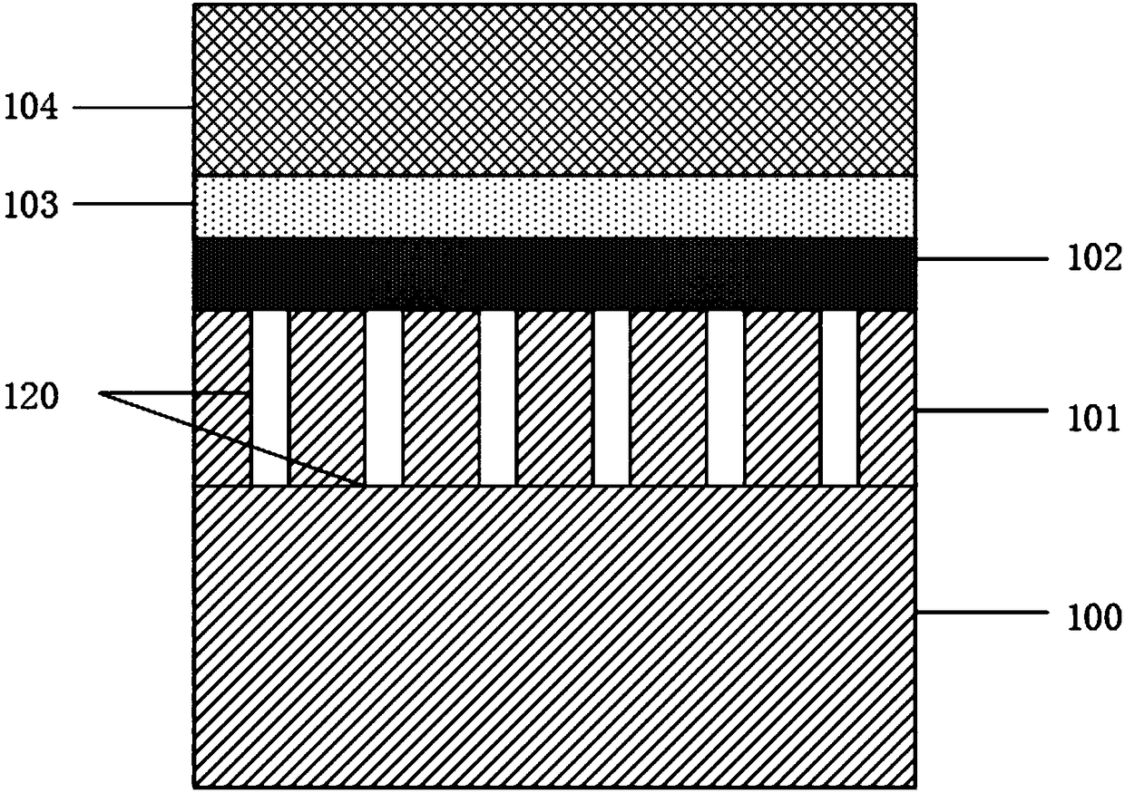
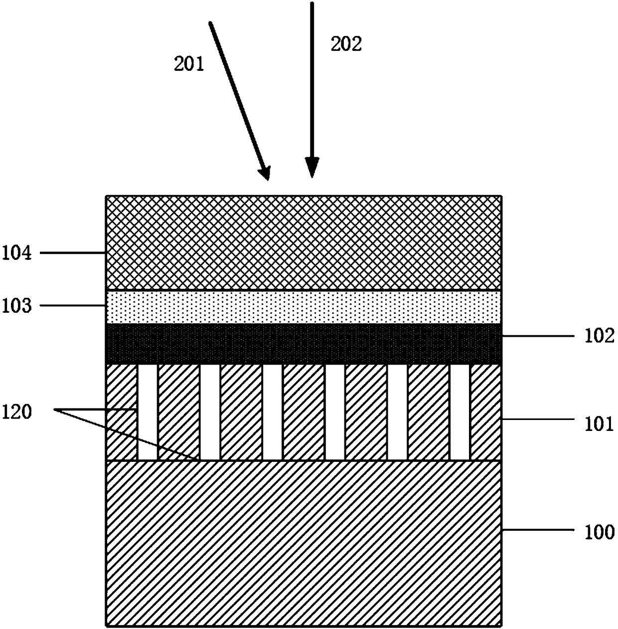
[0048] (1) On the substrate, a single crystal silicon material is deposited, and nanoholes are etched on the single crystal silicon material to form silicon photonic crystals. The radius of the nanoholes is 50nm, the distance between the holes is 700nm, and the hole depth is 150nm;

[0049] (2) Deposit a layer of SiO with a thickness of 15nm above the silicon photonic crystal 2 film;

[0050] (3) Deposit a layer of 5nm GeTe on the top of the isolation layer film;

[0051] (4) On top of the chalcogenide phase change material film, deposit a layer of SiN with oxidation resistance of 20nm x film, to obtain an all-optical switch. Etching is electron beam lithography and deposition is chemical vapor deposition.

Embodiment 2

[0053] A method for preparing an all-optical switch based on a chalcogenide phase-change material, comprising:

[0054] (1) On the substrate, a single crystal silicon material is deposited, and nanoholes are etched on the single crystal silicon material to form silicon photonic crystals. The radius of the nanoholes is 90nm, the distance between the holes is 850nm, and the hole depth is 250nm;

[0055] (2) Deposit a layer of SiO with a thickness of 40nm above the silicon photonic crystal 2 film;

[0056] (3) Deposit a layer of 25nm SbTe above the isolation layer film;

[0057] (4) On top of the chalcogenide phase change material film, deposit a layer of 200nm SiO with oxidation resistance 2 film, to obtain an all-optical switch. Etching is electron beam lithography and deposition is radio frequency magnetron sputtering.

Embodiment 3

[0059] A method for preparing an all-optical switch based on a chalcogenide phase-change material, comprising:

[0060] (1) On the substrate, a single crystal silicon material is deposited, and nanoholes are etched on the single crystal silicon material to form silicon photonic crystals. The radius of the nanoholes is 70nm, the distance between the holes is 800nm, and the hole depth is 200nm;

[0061] (2) Deposit a layer of SiN with a thickness of 30nm above the silicon photonic crystal x film;

[0062] (3) Deposit a layer of 15nm Bi on top of the isolation layer film 2 Te 3 ;

[0063] (4) Deposit a layer of 100nm SiO with oxidation resistance on top of the chalcogenide phase change material film 2 / ZnS film to obtain an all-optical switch. The etching is ion-coupled plasma etching, and the deposition is DC magnetron sputtering.


PUM

PropertyMeasurementUnit
radiusaaaaaaaaaa
thicknessaaaaaaaaaa
thicknessaaaaaaaaaa

Abstract

The invention discloses an all-optical switch based on a sulfur phase-change material and a preparation method thereof, and belongs to the field of optical communication. The all-optical switch comprises a coverage layer film, a sulfur phase-change material film, an isolation layer film, a silicon photonic crystal and a substrate which are sequentially stacked. The silicon photonic crystal comprises a nanometer porous structure, and the silicon photonic crystal has the fano resonance effect. When the all-optical switch is in use, the state of the sulfur phase-change material film is controlledthrough laser, the resonance state of the silicon photonic crystal is regulated, the signal light transmissivity is modulated, the modulation range is the communication wave band being 1,500 nanometers to 1,600 nanometers, and the optical switch is obtained. The all-optical switch has the advantages of being high in contrast ratio and speed and low in power consumption. The structure is simple, the production cost can be lowered, and the switch is suitable for CMOS integrated, capable of being easily matched with a modern semiconductor technology production line, and applicable to industrialproduction and productization.

Description

technical field [0001] The invention belongs to the field of optical communication, and more specifically relates to an all-optical switch based on a chalcogenide phase-change material and a preparation method thereof. Background technique [0002] Communication in modern society is mainly carried by optical fiber communication. However, due to the rapid development of the Internet and the emergence of new technologies such as the Internet of Things, people have higher requirements for the transmission rate of optical fiber communication. In the current traditional optical fiber communication system, there are a large number of optical interconnection and switching devices at the nodes. These devices have a large number of photoelectric to optical conversions. Due to the existence of electronic bottlenecks, this photoelectric conversion process will actually reduce the rate of optical fiber communication. Therefore, many scholars and experts have proposed the concept of all-...

Claims


Application Information

Patent Timeline
Patent Type & Authority Applications(China)
IPC IPC(8): G02F1/01G02F1/00G02B1/00
CPCG02F1/0063G02F1/0126G02B1/005G02B2207/101G02F2202/32G02F2202/36
Inventor 缪向水卢轶韬童浩汪毅
Owner HUAZHONG UNIV OF SCI & TECH
Why Eureka
Try Eureka