Germanium single crystal wafer and manufacturing method thereof, crystal rod manufacturing method and use of single crystal wafer

A germanium single wafer, germanium single crystal technology, applied in the direction of single crystal growth, single crystal growth, crystal growth, etc., can solve the problems of reducing the photoelectric conversion efficiency and open circuit voltage of batteries

Active Publication Date: 2018-05-29
BEIJING TONGMEI XTAL TECH CO LTD
View PDF7 Cites 9 Cited by
  • Summary
  • Abstract
  • Description
  • Claims
  • Application Information

AI Technical Summary

Problems solved by technology

However, when epitaxially growing III-V epitaxial materials on a germanium substrate, antiphase domains will be formed on the interface between the germanium substrate as the bottom cell and the epitaxial layer, and the boundaries of the formed antiphase domains will become photogenerated carriers. The recombination center reduces the photoelectric conversion efficiency and open circuit voltage of the battery

Method used


Image

  • Germanium single crystal wafer and manufacturing method thereof, crystal rod manufacturing method and use of single crystal wafer
  • Germanium single crystal wafer and manufacturing method thereof, crystal rod manufacturing method and use of single crystal wafer
  • Germanium single crystal wafer and manufacturing method thereof, crystal rod manufacturing method and use of single crystal wafer

Examples


preparation example Construction

[0123] In the method for preparing germanium single crystal rods of the present invention, the atomic concentration of silicon in the effective length of germanium single crystal rods is preferably 2×10 14 atoms / cc to 8×10 18 atoms / cc, more preferably 3×10 14 atoms / cc up to 7×10 18 atoms / cc; and the atomic concentration of gallium is preferably 2×10 16 atoms / cc to 9×10 19 atoms / cc, more preferably 2×10 16 atoms / cc to 8×10 19 atoms / cc.

[0124] Alternatively, in the method for preparing a germanium single crystal rod of the present invention, the atomic concentration of silicon within the effective length of the germanium single crystal rod is 1-25ppm based on the amount of germanium, and the atomic concentration of gallium is based on the amount of germanium 1-100ppm.

[0125] Alternatively, in the method for preparing a germanium single crystal rod of the present invention, the atomic concentration of silicon within the effective length of the germanium single crystal ...

Embodiment 1

[0224] Use 10kg bulk high-purity germanium raw material, 0.5g dopant gallium (50 ppm based on high-purity germanium raw material) and diboron trioxide liquid sealing agent.

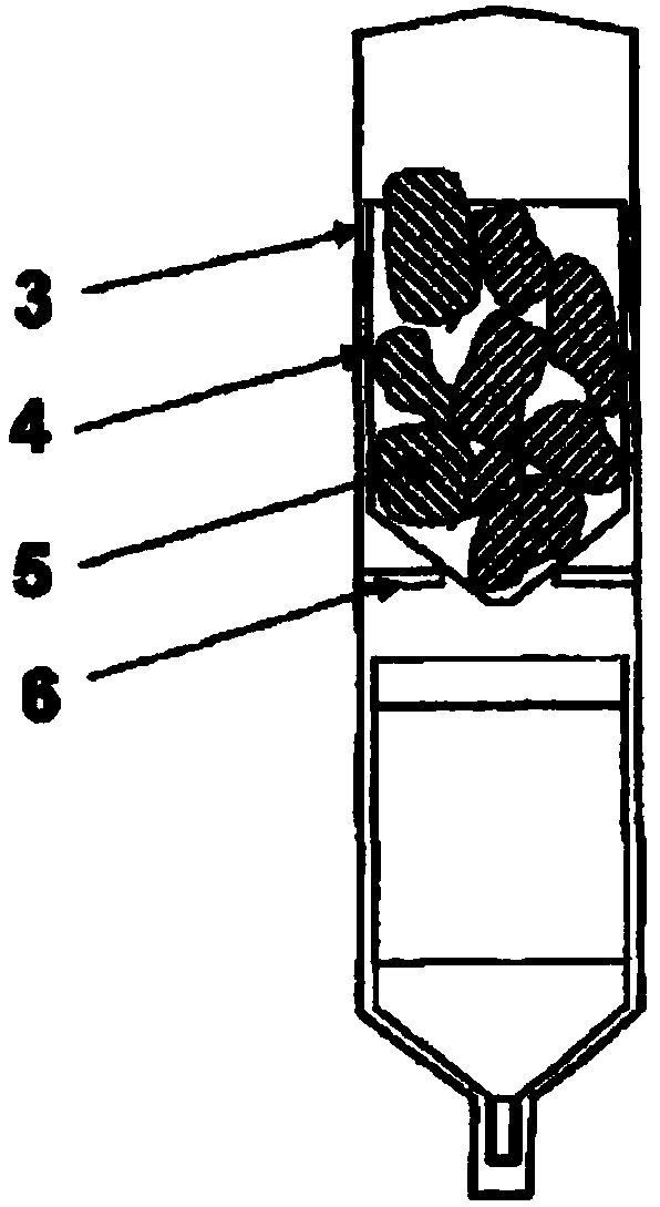
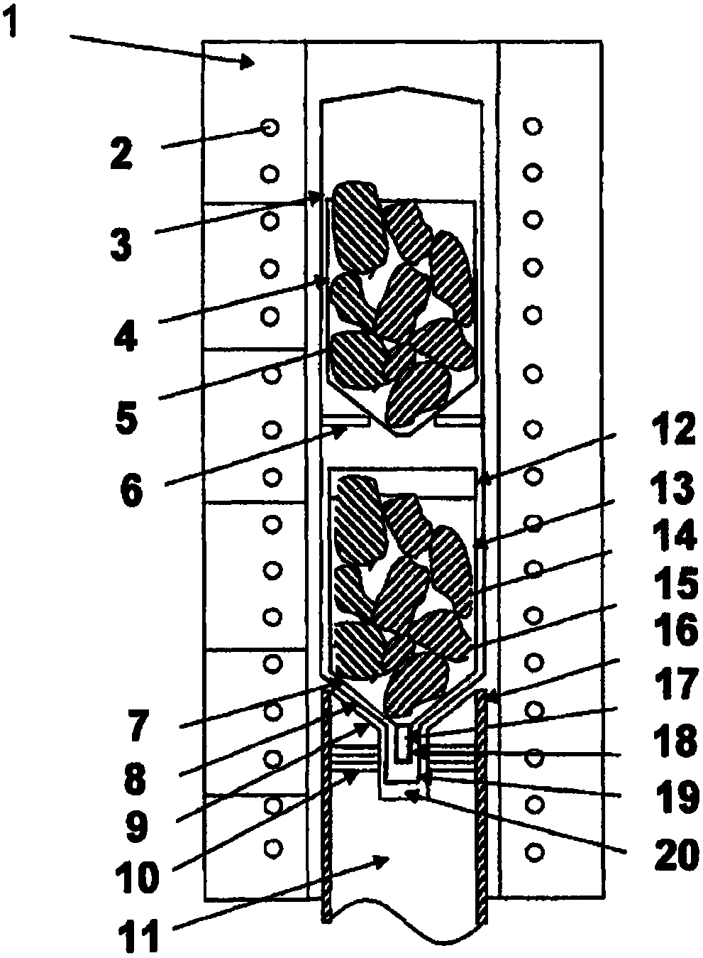
[0225] 1) 65% of the above-mentioned amounts of massive high-purity germanium, gallium, and diboron trioxide are respectively loaded into the first growth crucible, and the seed crystal groove of the first growth crucible is pre-installed with seeds;

[0226] 2) Put the remaining 35% of high-purity germanium and gallium into the second feeding crucible above the first growth crucible;

[0227] 3) Put the first growth crucible and the second feeding crucible into the quartz tube, and put them under vacuum at 10 -5 Sealed quartz tube under the condition of Torr;

[0228] 4) Put the quartz tube sealed with the first growth crucible and the second feeding crucible obtained in step 3) into a crystal growth furnace with a movable quartz tube support, which is used to support the quartz tube;

[0229] 5) Start...

Embodiment 2

[0233] Use 10kg bulk high-purity germanium raw material, 0.5g dopant gallium (50ppm based on high-purity germanium raw material), 0.01g dopant silicon (1ppm based on high-purity germanium raw material) and diboron trioxide liquid sealant .

[0234] 1) 65% of the above-mentioned amounts of massive high-purity germanium, gallium, silicon, and boron trioxide are respectively loaded into the first growth crucible, and the seed crystal groove of the first growth crucible is pre-installed with seeds;

[0235] 2) Put the remaining 35% of high-purity germanium, gallium, silicon and boron trioxide into the second feed crucible above the first growth crucible;

[0236] 3) Put the first growth crucible and the second feeding crucible into the quartz tube, and put them under vacuum at 10 -5 Sealed quartz tube under the condition of Torr;

[0237]4) Put the quartz tube sealed with the first growth crucible and the second feeding crucible obtained in step 3) into a crystal growth furnace ...


PUM

PropertyMeasurementUnit
thicknessaaaaaaaaaa
particle diameteraaaaaaaaaa
surface smoothnessaaaaaaaaaa

Abstract

The invention relates to a germanium (Ge) single crystal wafer used for increasing open-circuit voltages of multi-cell solar batteries, a manufacturing method of the germanium single crystal wafer, and a manufacturing method of a crystal rod used for preparing the germanium single crystal wafer. By adjusting the amount of co-doping element silicon and germanium in the germanium single crystal wafer, a proportion of the co-doping element silicon and germanium when a germanium single crystal rod used for increasing the open-circuit voltages of the multi-cell solar batteries is prepared, as wellas the rate of growth and the temperature gradient of the germanium single crystal, the germanium single crystal wafer capable of increasing battery open-circuit voltages of multi-stage solar batteries is prepared.

Description

technical field [0001] The invention relates to a germanium (Ge) single chip for increasing the open-circuit voltage of multiple solar cells, a preparation method for a germanium single chip for increasing the open-circuit voltage of multiple solar cells, and a method for preparing a crystal bar for increasing the open-circuit voltage of multiple solar cells for a germanium single chip. Background technique [0002] High-efficiency and high-power solar cells have been widely used in space solar systems and large-scale ground-based concentrated solar systems. The germanium single wafer is the ideal substrate material for this high-efficiency and high-power multi-cell solar cell, and the germanium substrate material is the material for the bottom cell of the multi-cell solar cell. Compared with the 15-20% photoelectric conversion efficiency of silicon-based single-junction solar cells, the conversion efficiency of germanium-based multi-junction solar cells is greatly increased...

Claims


Application Information

Patent Timeline
Patent Type & Authority Applications(China)
IPC IPC(8): H01L31/0288H01L31/18C30B13/00C30B29/08
CPCC30B13/00C30B29/08H01L31/0288H01L31/1828C30B11/00H01L31/0687H01L31/0693H01L31/1852Y02E10/543Y02E10/544C30B11/006C30B33/00
Inventor 拉贾拉姆·谢蒂王元立周雯婉刘卫国朱颂义
Owner BEIJING TONGMEI XTAL TECH CO LTD
Why Eureka
Try Eureka