Integrated drug screening and staining dyeing micro-fluidic chip and preparation method thereof
A microfluidic chip and drug technology, applied in the field of processing, microfluidic technology and polymer chip design, production and application, can solve the problems of cumbersome and complicated operation steps and large consumption, and achieve wide application range and convenient operation , high efficiency effect
- Summary
- Abstract
- Description
- Claims
- Application Information
AI Technical Summary
Problems solved by technology
Method used
Image
Examples
Embodiment 1
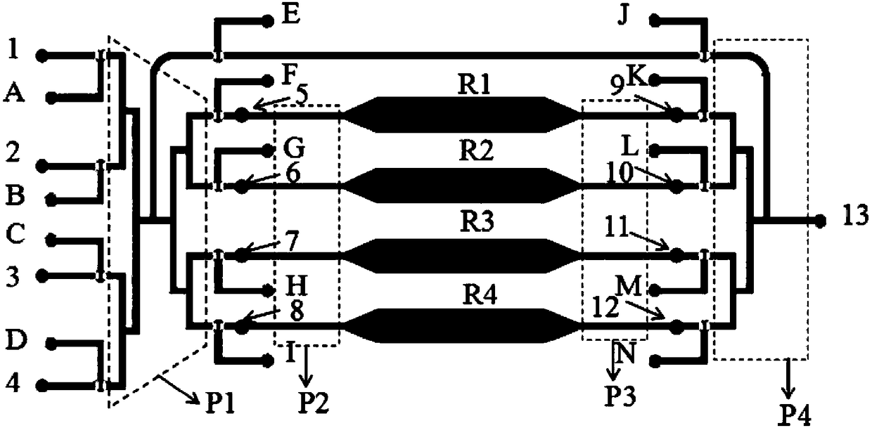
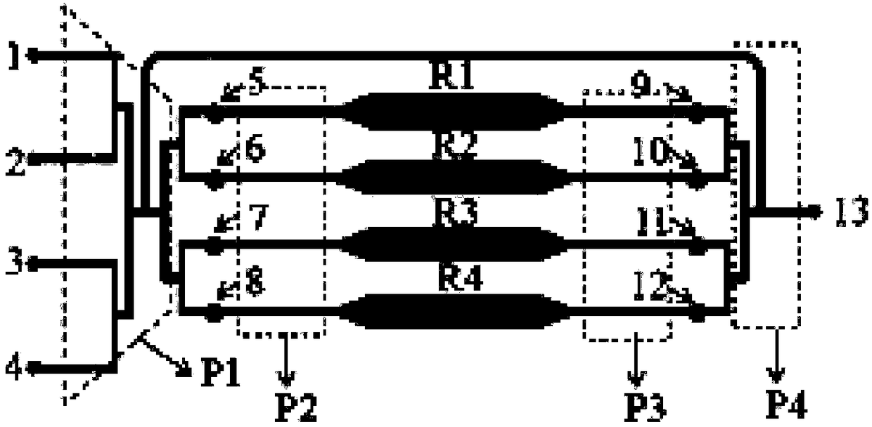
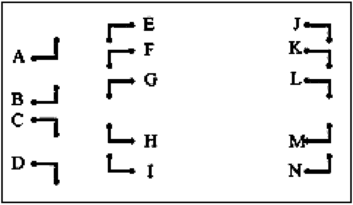
[0055] An integrated drug screening and dyeing microfluidic chip, the microfluidic chip is composed of an upper layer, a lower layer, and a bottom layer sequentially laminated in series, wherein: the upper layer is a liquid circuit control layer, and the lower layer is a gas circuit control layer, The bottom surface is a blank glass bottom plate;
[0056] The liquid path control layer is specifically provided with the following structure:
[0057] ——Cell fluorescence staining inlet: located at the most upstream of the entire liquid path control layer; it is provided with at least two channels with its inlets parallel to each other and finally merged into a common channel; the finally merged shared channel is also respectively connected to the downstream cell culture chamber and the liquid outflow channel;
[0058] ——Fluorescence dyeing injection channel area (P1): arranged between the cell fluorescence dyeing injection port and the cell injection channel area (P2) for communi...
Embodiment 2
[0092] The integrated drug screening and dyeing chip adopts photolithography and etching methods to prepare SU-8 templates with channel protrusions. The upper and lower structures of the chip are respectively composed of two SU-8 template anti-mold PDMS; two SU-8 templates are produced at the same time, Take two pieces of clean glass, throw the SU-8 adhesive on the adhesive machine to a thickness of 100 μm, pre-bake at 95°C for 20 minutes, cool down naturally, place the two masks of the upper and lower layers of the chip on the SU-8 adhesive plate, and UV Expose for 30s, bake at 95°C for 20min, and cool down naturally; finally, use ethyl lactate to develop the above SU-8 gel for 5min, harden the film at 180°C for 2h, and cool down naturally to obtain a chip template.
Embodiment 3
[0094] Treat the SU-8 template of the lower structure of the chip with a silylating agent for 10 minutes, so that PDMS can be easily peeled off the bottom surface of the template; PDMS and initiator are mixed evenly at a volume ratio of 10:1, and poured on the SU-8 template of the upper and lower structures of the chip respectively, 80 Cure in an oven for 40 minutes, peel off the PDMS and the SU-8 template on the upper layer of the chip, and obtain a PDMS chip with a structure; perform oxygen plasma treatment on the side with the structure on the upper layer of the chip and the lower layer of the chip without a structure on the SU-8 template for 2 minutes , baked at 80°C for 1 hour, and irreversibly sealed; peeled off the sealed PDMS chip from the SU-8 template of the underlying structure, treated with oxygen plasma for 2 minutes with a clean blank glass sheet, and baked at 80°C for 1 hour for irreversible sealing , that is, an integrated drug screening and dyeing microfluidic ...
PUM
 Abstract
Description
Claims
Application Information


