Field effect transistor based on negative capacitance and preparation method thereof, and biosensor and preparation method thereof

A field-effect transistor and negative capacitance technology, which is applied in transistors, semiconductor/solid-state device manufacturing, semiconductor devices, etc., can solve the problems of high subthreshold swing, low sensitivity and response speed, high device power, etc., and achieve excellent ferroelectric performance , Improve the sensing sensitivity and response speed, and the effect of simple process

Inactive Publication Date: 2018-06-29
SHANGHAI INST OF MICROSYSTEM & INFORMATION TECH CHINESE ACAD OF SCI
View PDF4 Cites 21 Cited by
  • Summary
  • Abstract
  • Description
  • Claims
  • Application Information

AI Technical Summary

Problems solved by technology

[0007] In view of the shortcomings of the prior art described above, the purpose of the present invention is to provide a field effect transistor structure based on negative capacitance, a biosensor and a preparation method thereof, which are used to solve the problem of high sub-threshold swing, sensitivity and response in the prior art. Issues such as low speed and high device power

Method used


Image

  • Field effect transistor based on negative capacitance and preparation method thereof, and biosensor and preparation method thereof
  • Field effect transistor based on negative capacitance and preparation method thereof, and biosensor and preparation method thereof
  • Field effect transistor based on negative capacitance and preparation method thereof, and biosensor and preparation method thereof

Examples


Embodiment 1

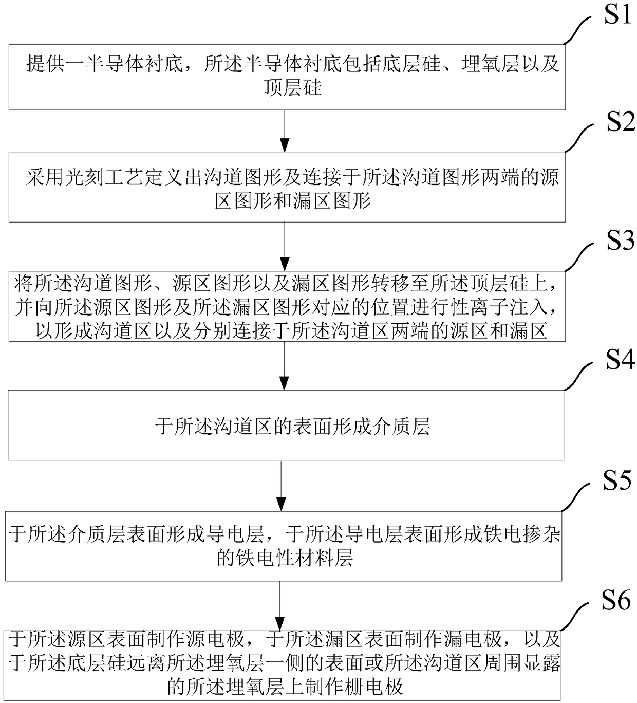
[0076] Such as Figure 1-9 As shown, the present invention provides a kind of preparation method based on the field effect transistor of negative capacitance, comprises the steps:

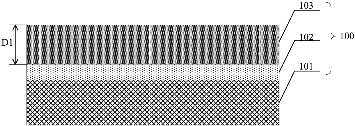
[0077] 1) providing a semiconductor substrate, said semiconductor substrate comprising bottom silicon, buried oxide layer and top silicon;

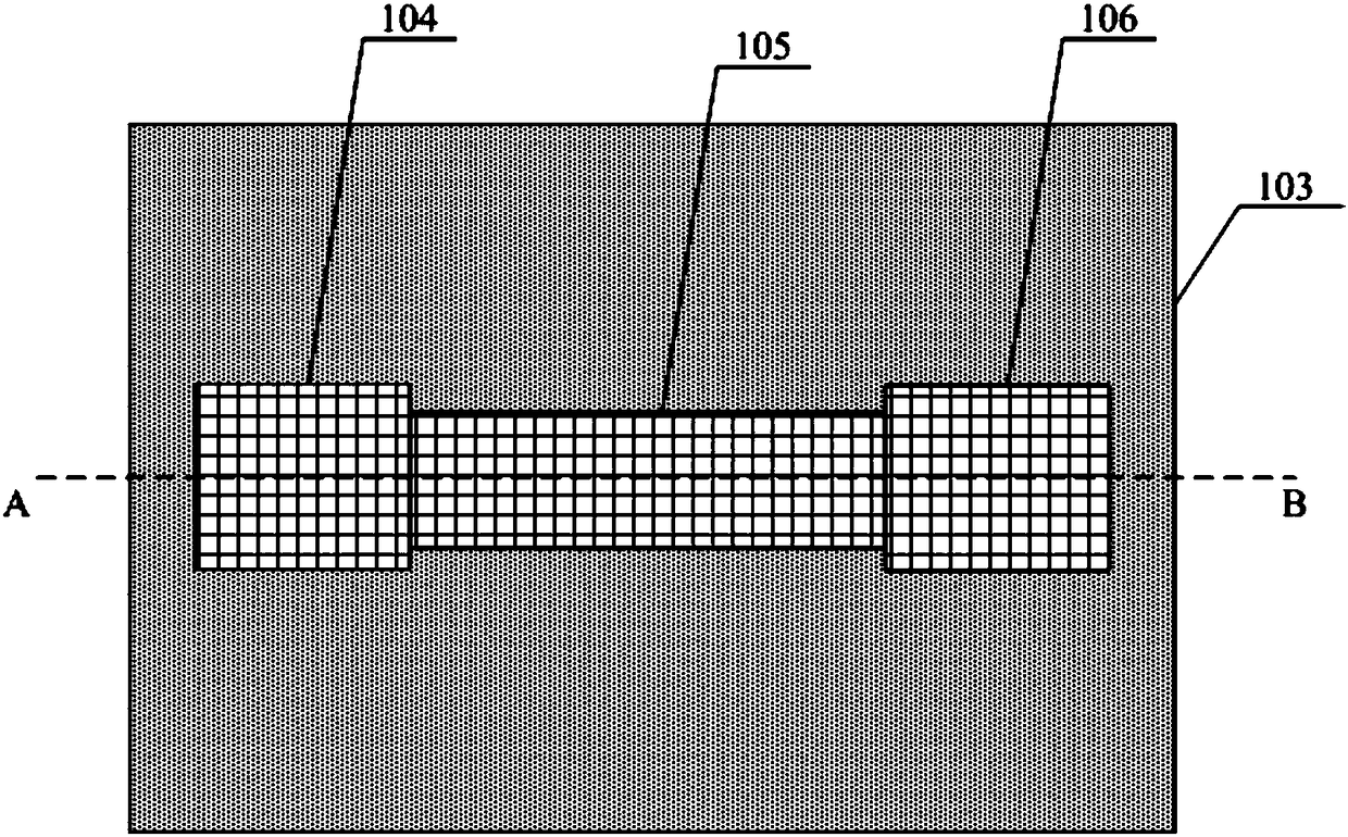
[0078] 2) using a photolithography process to define a channel pattern and a source region pattern and a drain region pattern connected to both ends of the channel pattern;

[0079] 3) Transferring the channel pattern, source region pattern and drain region pattern to the top layer of silicon, and performing ion implantation to the positions corresponding to the source region pattern and the drain region pattern to form a channel region and a source region and a drain region respectively connected to two ends of the channel region;

[0080] 4) forming a dielectric layer on the surface of the channel region;

[0081] 5) forming a conductive layer on the surf...

Embodiment 2

[0126] Such as Figure 10 As shown, the present invention also provides a method for preparing a biosensor, comprising the steps of:

[0127] 1) adopt the preparation method as described in any one scheme in embodiment one to prepare the field-effect transistor based on negative capacitance;

[0128] 2) using a reagent to modify the surface of the channel region of the field effect transistor to form an active film terminated with an active group; and

[0129]3) forming a capture probe on the surface of the active film, wherein the capture probe is combined with an active group on the active film through a chemical bond, so that the capture probe is modified in the silicon nanowire groove the surface of the road.

[0130] As an example, the active group includes one or a combination of two or more of amino group, carboxyl group, hydroxyl group and aldehyde group, which is set according to actual needs.

[0131] Specifically, the present invention also provides a biosensor b...


PUM

PropertyMeasurementUnit
thicknessaaaaaaaaaa
thicknessaaaaaaaaaa
thicknessaaaaaaaaaa

Abstract

The present invention provides a field effect transistor based on negative capacitance and a preparation method thereof, and a biosensor and a preparation method thereof. The preparation method of thefield effect transistor comprises the steps of: providing a semiconductor substrate comprising underlying silicon, buried oxide and top silicon; defining a channel figure, and a source figure and a drain figure which are connected with two ends; performing ion implantation to positions corresponding to the source figure and the drain figure to form a channel region, a source region and a drain region; forming a dielectric layer at the surface of the channel region; forming a conductive layer at the surface of the dielectric layer, and forming a ferroelectricity material layer at the surface of the conductive layer; and making a source electrode, a drain electrode and a gate electrode. According to the scheme, a traditional field effect transistor is integrated with the ferroelectricity negative capacitance to reduce the subthreshold amplitude of a device, improve the sensing sensitivity and the response speed and facilitate reduction of the device power; and moreover, the ferroelectric-doping hafnium oxide is taken as a ferroelectric negative capacitance medium so as to solve the problem that inorganic ferroelectric materials are difficult to a CMOS technology.

Description

technical field [0001] The invention belongs to the technical field of semiconductor device manufacturing, and in particular relates to a negative capacitance-based field effect transistor, a biosensor and a preparation method. Background technique [0002] Today in the 21st century, science and technology have made great progress, but environmental pollution, food pollution, and malignant diseases still seriously threaten human health and survival. Biochemical molecular sensing technology can capture the information of the environment, food and organisms, and provide technical support for environmental monitoring, food analysis, clinical medical diagnosis, biomedical research, etc. [0003] As a new type of semiconductor sensing technology, semiconductor field effect transistor has the advantages of high sensitivity, easy integration, and low cost, and it opens up a comprehensive way for the rapid and sensitive detection of biochemical molecules. Sub-threshold swing (Sub-t...

Claims


Application Information

Patent Timeline
Patent Type & Authority Applications(China)
IPC IPC(8): H01L29/78H01L21/336G01N27/414
CPCG01N27/4145H01L29/66568H01L29/78391
Inventor 高安然韩清华赵兰天赵清太李铁王跃林
Owner SHANGHAI INST OF MICROSYSTEM & INFORMATION TECH CHINESE ACAD OF SCI
Why Eureka
Try Eureka