Method for preparing 2D perovskite quantum well film with high gain property
A quantum well thin film and perovskite technology, applied in chemical instruments and methods, 4/14 group organic compounds without C-metal bonds, lead organic compounds, etc., can solve problems such as radiation decay and low energy band gap, and achieve Improved stability, good optical absorption performance, and uniform shape
- Summary
- Abstract
- Description
- Claims
- Application Information
AI Technical Summary
Problems solved by technology
Method used
Image
Examples
Embodiment 1
[0057] In the present embodiment, the preparation method of 2D perovskite quantum well film comprises the following steps:
[0058] 1) Butylamine bromide and lead dibromide are dissolved in anhydrous dimethyl sulfoxide (DMSO) at a molar ratio of 2:1, heated and ultrasonicated until the solid is completely dissolved to form 2D butylamine lead bromide (BA) 2 PbBr 4 Perovskite precursor solution;
[0059] 2) Dissolving methylamine bromide and lead dibromide in anhydrous dimethyl sulfoxide (DMSO) at a ratio of 1:1 to form a precursor solution of 3D methylamine lead bromine perovskite;
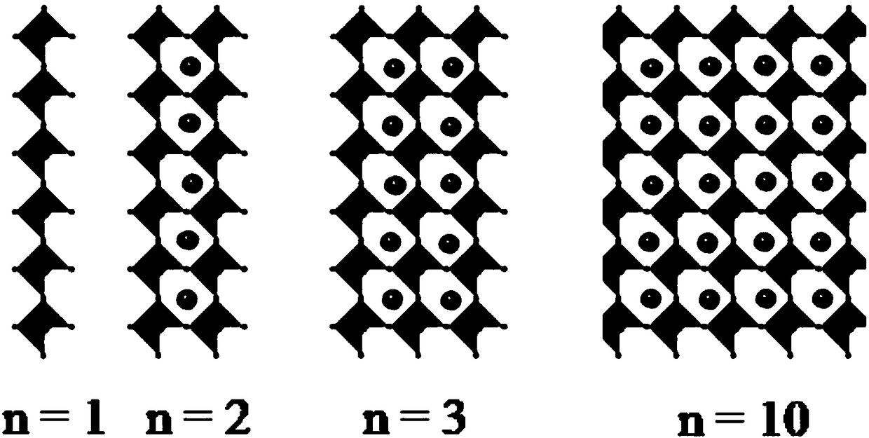
[0060] 3) Finally, the two perovskite precursor solutions were mixed in equal volumes to obtain a 2D perovskite quantum well material (BA) 2 (MA)Pb 2 Br 7 (n=2) precursor solution;
[0061] 4) Use a pipette gun to take 100 μL of the precursor solution of the 2D perovskite quantum well material and drop it on a piece of glass substrate. A bulk solvent was used to obtain a 2D perovskite quantum...
Embodiment 2
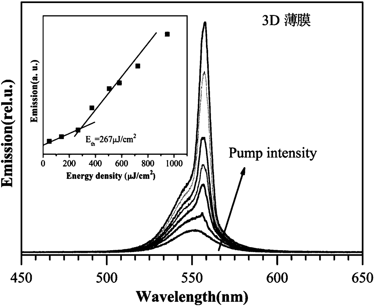
[0064] Step is as embodiment one, and methylamine bromide and lead dibromide are changed into methylammonium iodide and lead diiodide, and other conditions are unchanged. The position of the emission spectrum of the obtained film is at 600nm, the thickness of the film is ~100nm, the thickness is ~2nm, and the gain coefficient is 320cm -1 , with high gain characteristics.
Embodiment 3
[0066] 1) Dissolve butylamine iodine and lead diiodide in anhydrous N-N dimethylformamide (DMF) at a molar ratio of 2:1, heat and sonicate until the solid is completely dissolved to form 2D butylamine iodine (BA) 2 PB 4 Perovskite precursor solution;
[0067] 2) Dissolve methylamine iodide and lead diiodide in anhydrous N-N dimethylformamide (DMF) at a molar ratio of 2:2 to form 3D methylamine lead iodide MAPbI 3 Perovskite precursor solution;
[0068] 3) Finally, the two perovskite precursor solutions were mixed in equal volumes to obtain a 2D perovskite quantum well material (BA) 2 (MA) 2 Pb 3 I 10 (n=3) precursor solution;
[0069] 4) Use a pipette gun to take 50 μL of the precursor solution of the 2D perovskite quantum well material and drop it on a sapphire substrate. A bulk solvent was used to obtain a 2D perovskite quantum well film with a thickness of 350 nm.
[0070] Among them, the position of the emission spectrum is at 620nm, the coarseness is ~6nm, and the...
PUM
| Property | Measurement | Unit |
|---|---|---|
| thickness | aaaaa | aaaaa |
| Gain coefficient | aaaaa | aaaaa |
| emission peak | aaaaa | aaaaa |
Abstract
Description
Claims
Application Information


