

SMD-type IRM high shielding structure and making process thereof
A technology of shielding structure and manufacturing process, applied in semiconductor/solid-state device manufacturing, electrical components, electrical solid-state devices, etc., can solve the problems of many stent production processes, complex production processes, affecting the overall yield rate, etc., to reduce assembly difficulty and Labor cost, simple production process, and the effect of reducing waste water and waste gas pollution
- Summary
- Abstract
- Description
- Claims
- Application Information
AI Technical Summary
Problems solved by technology
Method used
Image

Examples
Embodiment Construction
[0032] The present invention is described in further detail now in conjunction with accompanying drawing. These drawings are all simplified schematic diagrams, which only illustrate the basic structure of the present invention in a schematic manner, so they only show the configurations related to the present invention.
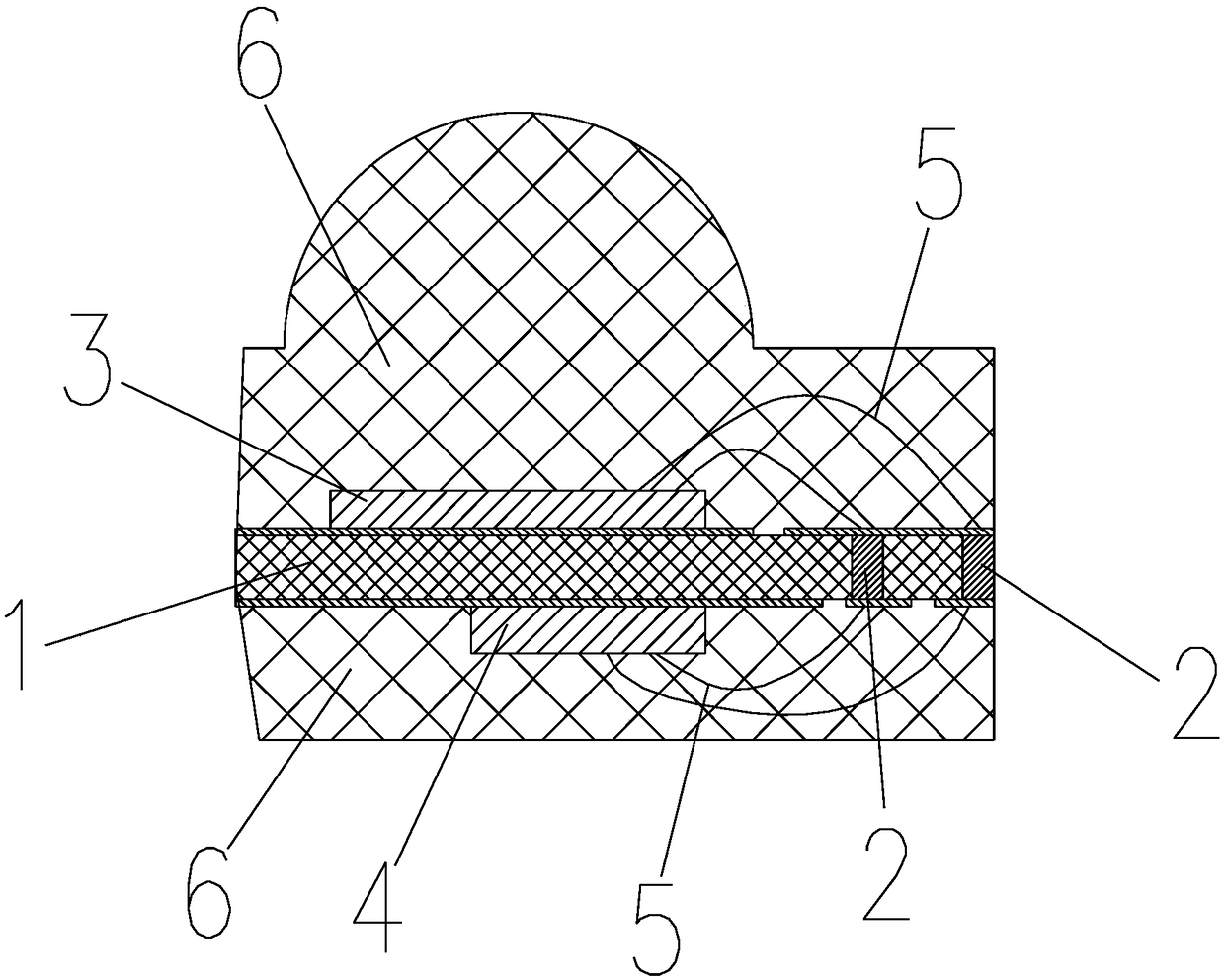
[0033] Such as figure 1 The specific embodiment of a kind of patch type IRM high shielding structure of the present invention shown, it comprises PCB board 1, is penetrated with several conduction holes on PCB board 1, is all plugged with copper column 2 in each conduction hole, The circuits on both sides of the PCB board 1 are conducted through the copper pillars 2; the front side of the PCB board 1 is provided with a PD chip 3, and the reverse side is provided with an IC chip 4; one end of each copper pillar 2 is connected to the PD chip through a bonding wire 5 3, the other end of each copper column 2 is connected to the IC chip 4 through the bonding wire ...
PUM
 Abstract
Description
Claims
Application Information