III-group nitride semiconductor avalanche photoelectric detector with absorption layer and multiplication layer separated structure

A nitride semiconductor and separation structure technology, applied in the field of photodetectors, can solve the problems of high probability of photogenerated holes and reduced quantum efficiency, and achieve the effects of high quantum efficiency, high avalanche gain, and increased electric field strength

Active Publication Date: 2018-07-20
SUN YAT SEN UNIV
View PDF7 Cites 13 Cited by
  • Summary
  • Abstract
  • Description
  • Claims
  • Application Information

AI Technical Summary

Problems solved by technology

Since the mean free path of holes in AlGaN materials, especially high Al composition AlGaN (Al composition is greater than 35%) is small (tens of nanometers), the photogenerated holes are in the layer when they cross the n-type doped charge layer. The probability of being recombined by electrons is high, resulting in a decrease in quantum efficiency

Method used


Image

  • III-group nitride semiconductor avalanche photoelectric detector with absorption layer and multiplication layer separated structure

Examples


Embodiment Construction

[0031] In order to make the object, technical solution and advantages of the present invention clearer, the present invention will be further described in detail below in conjunction with the accompanying drawings and specific implementation methods. It should be understood that the specific embodiments described here are only used to explain the present invention, and do not limit the protection scope of the present invention.

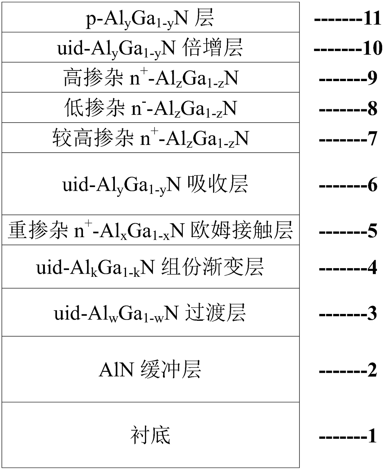
[0032] The structure and method are suitable for making an AlGaN ternary compound material ultraviolet avalanche photodetector based on absorption and multiplication layer separation, and the light signal is incident from one side of the substrate.

[0033] Such as figure 1 As shown, an AlGaN semiconductor avalanche photodetector with absorption, multiplication and separation structure, the device includes: a wurtzite structure single crystal sapphire substrate 1, using epitaxial growth methods, such as molecular beam epitaxy or metal organic chemical...


PUM


Abstract

The invention discloses a III-group nitride semiconductor avalanche photoelectric detector with an absorption layer and multiplication layer separated structure. The detector includes a substrate andepitaxial layers grown on the substrate, wherein the epitaxial layers include a AlN buffer layer, an unintentionally doped AlwGa1-wN transition layer, an unintentionally doped AlkGa1-kN composition graded layer, a heavily doped n type AlxGa1-xN ohmic contact layer, an unintentionally doped AlyGa1-yN absorption layer, a charge layer, an unintentionally doped AlyGa1-yN multiplication layer and a p type doped AlyGa1-yN layer which are grown sequentially from bottom to top, wherein the charge layer comprises at least three n type AlzGa1-zN layers, and the doping concentration of the charge layer is in high-low-high saddle type doping distribution. The III-group nitride semiconductor avalanche photoelectric detector has the advantages of improved performance, low noise, low working voltage, high gain and high quantum efficiency.

Description

technical field [0001] The invention relates to the field of photodetectors, in particular to a Group III nitride semiconductor avalanche photodetector with absorption and multiplication layer separation structure. Background technique [0002] With the increasing update of information technology, solid-state photodetection technology based on compound semiconductor materials plays an increasingly important role in the entire field of modern photoelectric information detection. In recent years, the application of photoelectric detection technology in national defense, civil and scientific fields has been increasing, such as flame detection, environmental monitoring, missile early warning, quantum communication, space optical communication, visible light infrared camera and so on. Compared with the traditional vacuum photodetection devices represented by photomultiplier tubes (PMTs), solid-state detection devices have the advantages of low operating voltage, high temperature ...

Claims


Application Information

Patent Timeline
Patent Type & Authority Applications(China)
IPC IPC(8): H01L31/107H01L31/0304
CPCH01L31/03048H01L31/1075
Inventor 江灏陈萌
Owner SUN YAT SEN UNIV
Why Eureka
Try Eureka