Hall sensor with local groove structure of two-dimensional electron gas channel barrier layer and its manufacturing method

A Hall sensor, two-dimensional electronic technology, applied in the direction of Hall effect devices, electromagnetic device manufacturing/processing, electromagnetic equipment components, etc. Effects of increased voltage drop, improved device sensitivity, high electron mobility

Active Publication Date: 2019-10-11
DALIAN UNIV OF TECH
View PDF2 Cites 0 Cited by
  • Summary
  • Abstract
  • Description
  • Claims
  • Application Information

AI Technical Summary

Problems solved by technology

[0003] However, there are still some problems in the existing semiconductor heterojunction Hall sensors. One of the main problems is that although the existence of the two-dimensional electron gas channel can significantly improve the electron mobility, due to the high In the electric field perpendicular to the direction of the channel (longitudinal electric field), the electrons are completely bound in the interface channel, and the ability of the Lorentz force in the Hall effect to drive the carriers away from the original lateral transport track is weakened, which leads to the sensing Reduced voltage or current sensitivity

Method used


Image

  • Hall sensor with local groove structure of two-dimensional electron gas channel barrier layer and its manufacturing method
  • Hall sensor with local groove structure of two-dimensional electron gas channel barrier layer and its manufacturing method
  • Hall sensor with local groove structure of two-dimensional electron gas channel barrier layer and its manufacturing method

Examples


Embodiment 1

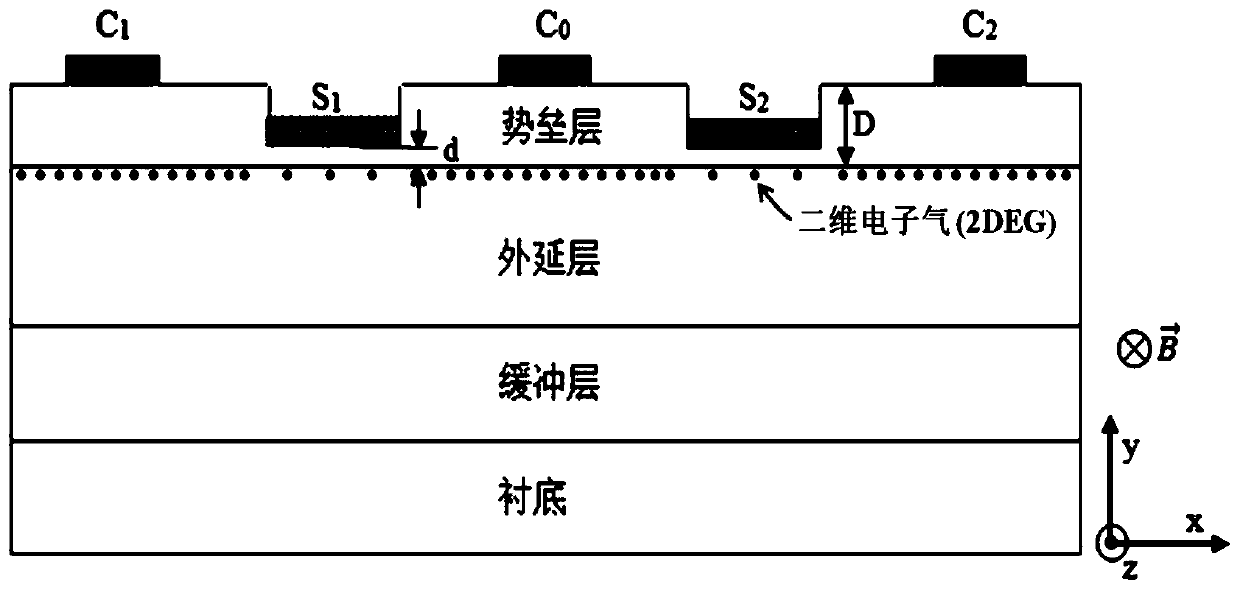
[0028] The structural schematic diagram of the technical solution of the present invention is as follows: figure 1 . Grow buffer layer, epitaxial layer and barrier layer respectively on a semiconductor substrate, the substrate is semiconductor or any other common substrate that can support semiconductor epitaxial growth, especially including Si, InAs, GaAs, SiC, GaN, ZnO, gallium oxide , boron nitride, diamond, sapphire, or any one of quartz, without special limitation; the epitaxial layer can be GaAs, GaN or SiC, without special limitation; the barrier layer can be AlGaAs, There is no special limitation on AlGaN (or InAlN or AlN), or AlN, and the material composition in the barrier layer is not particularly limited. All material combinations and parameter selections for semiconductor heterojunction structures that can generate two-dimensional electron gas are included in this paper. The scope of the patent is limited. The background carrier concentration range of epitaxial ...

Embodiment 2

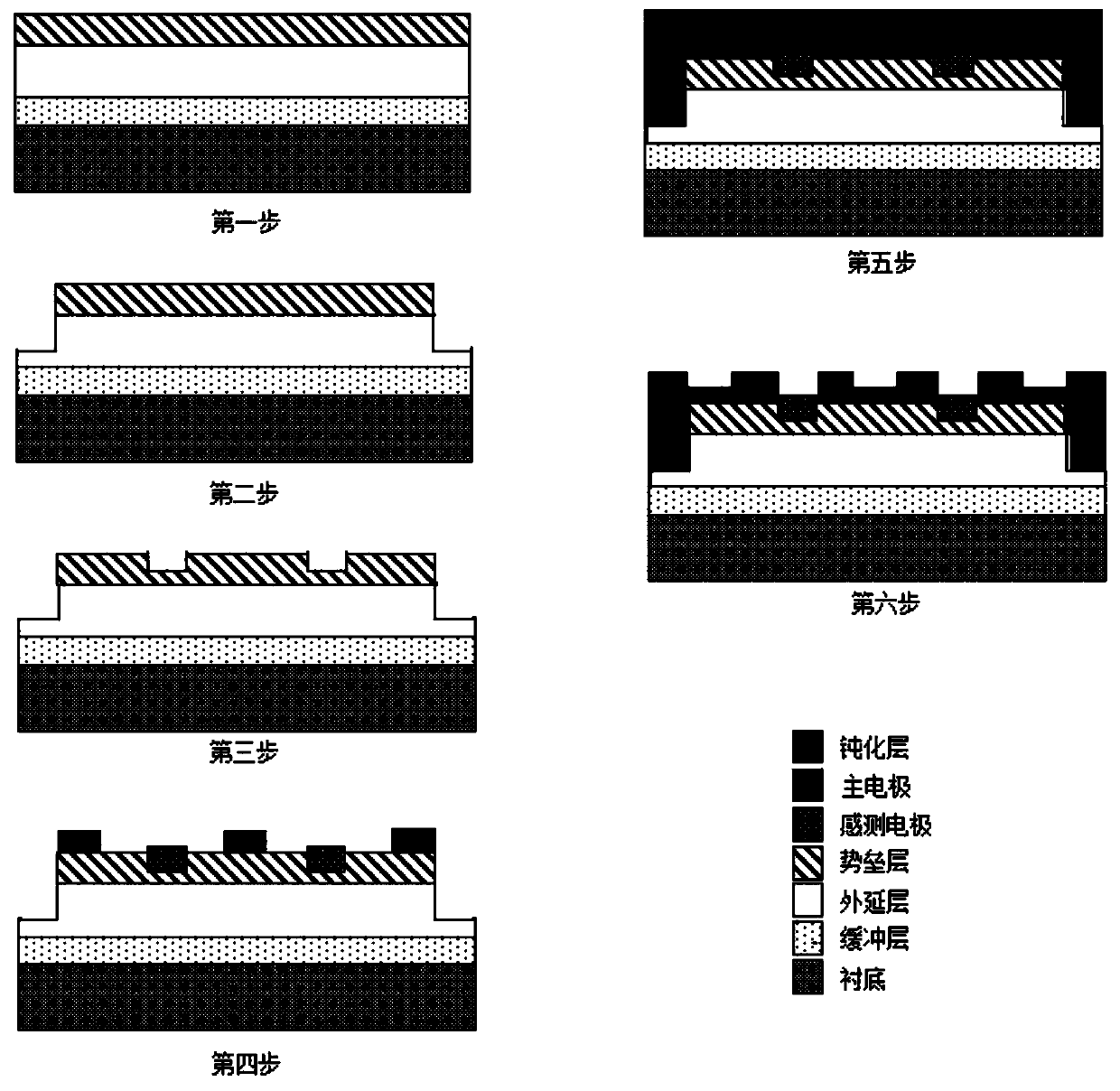
[0032] figure 2 Shows the basic process of making the Hall sensor proposed by the present invention:

[0033] Step 1: Device chip material preparation with heterojunction structure:

[0034] Device base material includes substrate, buffer layer, epitaxial layer and barrier layer. The device materials were ultrasonically cleaned with acetone, ethanol, and deionized water, each step was ultrasonically timed for 10 minutes, then dried with nitrogen, and baked in an oven at 110°C for 10 minutes for use.

[0035] The second step: device mesa etching and isolation:

[0036] The device mesa is defined by photolithography technology, and a good etching window is formed through steps such as glue coating, glue leveling, photolithography, and development, and then wet or dry etching technology is used to etch the material barrier layer and epitaxial layer. The etching depth is generally 20-2000nm.

[0037] Step 3: The barrier layer is selectively etched to form a local groove:

[...

Embodiment 3

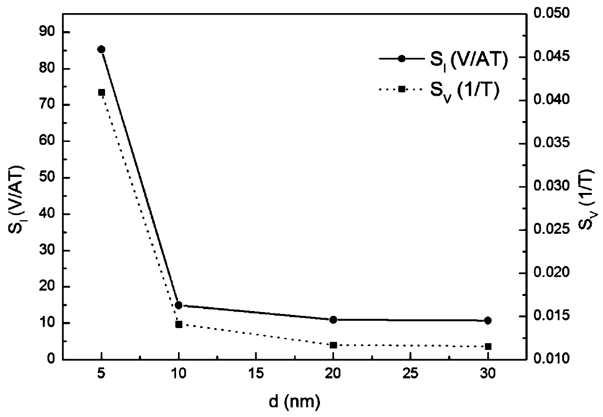
[0046] 1. Device structure parameters

[0047] A GaN material epitaxial wafer with Si substrate AlN as the buffer layer was used, in which the epitaxial layer was unintentionally doped GaN with a thickness of 6 μm and a background electron concentration of 1×10 16 cm -3 , the barrier layer is AlGaN, the thickness is 30nm, and the Al composition is 0.25. The three main electrodes of the chip C 0 、C 1 and C 2 and the Hall sensing electrode S on the groove 1 and S 2 The width is 2μm, where the electrode C 0 with electrode C 1 、C 2 The spacing is 8μm, the electrode C 0 with electrode S 1 , S 2 The pitches are all 3.5 μm.

[0048] 2. Device manufacturing process

[0049] Step 1: Device chip material preparation with heterojunction structure:

[0050] The device materials were ultrasonically cleaned with acetone, ethanol, and deionized water, each step was ultrasonically timed for 10 minutes, then dried with nitrogen, and baked in an oven at 110°C for 10 minutes for us...


PUM


Abstract

A Hall sensor with a local groove structure of a two-dimensional electron gas channel barrier layer and a manufacturing method thereof, belonging to the field of semiconductor sensors. A buffer layer, an epitaxial layer and a barrier layer are sequentially grown on the semiconductor substrate, and three main electrodes C are arranged on the surface of the barrier layer. 0 、C 1 and C 2 , main electrode C 1 and C 2 About the main electrode C 0 Centrosymmetric, main electrode C 0 and C 1 Between, C 0 and C 2 There is a groove structure between them, and the groove structure on both sides is about the main electrode C 0 Centrosymmetric, and the width of the groove structure is less than C 0 and C 1 or C 0 and C 2 Inter-electrode spacing, main electrode C 0 and C 1 Sensing electrodes S are arranged on the groove structure between 1 , main electrode C 0 and C 2 Sensing electrodes S are arranged on the groove structure between 2 . The invention forms grooves by shallow etching in selected areas, retains the intact heterojunction interface under the grooves, can take advantage of the high mobility of two-dimensional electron gas, and can ensure that the carriers in motion under weak magnetic field signals can generate effectively offset, thereby increasing the detection sensitivity of the device.

Description

technical field [0001] The invention relates to the field of semiconductor sensors, in particular to a Hall sensor with a local groove structure of a two-dimensional electron gas channel barrier layer and a manufacturing method thereof. Background technique [0002] The Hall magnetic field sensor is currently one of the most widely used sensor types for detecting the magnitude of the magnetic field, and has been widely used in biomedicine, automotive electronics, space detection and other fields. One of the important indicators for evaluating device performance in Hall sensors is voltage or current sensitivity, and this indicator is mainly restricted by the mobility of material carriers. The higher the mobility, the higher the sensitivity of the device. There are two basic structures of materials for existing semiconductor Hall sensors, one is based on a uniform single body material, and the other is based on III-V semiconductor heterojunctions represented by AlGaN / GaN and A...

Claims


Application Information

Patent Timeline
Patent Type & Authority Patents(China)
IPC IPC(8): H01L43/06H01L43/04H01L43/14
CPCH10N52/80H10N52/01H10N52/101
Inventor 黄火林曹亚庆李飞雨孙仲豪
Owner DALIAN UNIV OF TECH
Why Eureka
Try Eureka