Single-crystal-silicon surface mechanical damage detecting method based on conductivity variation

A technology of mechanical damage and detection methods, which is applied in the direction of measuring devices, instruments, scanning probe microscopy, etc., can solve the problems of difficult to adjust the detection position in time, the detection process and results are out of sync, and the sample preparation process is complicated, etc. The results are online controllable, low cost and high efficiency

Inactive Publication Date: 2018-07-27
SOUTHWEST JIAOTONG UNIV
View PDF6 Cites 1 Cited by
  • Summary
  • Abstract
  • Description
  • Claims
  • Application Information

AI Technical Summary

Problems solved by technology

The sample preparation process of these methods is usually relatively complicated, and the sample preparation process for transmission electron microscopy detection will cause damage to the sample, and only local detecti...

Method used


Image

  • Single-crystal-silicon surface mechanical damage detecting method based on conductivity variation
  • Single-crystal-silicon surface mechanical damage detecting method based on conductivity variation
  • Single-crystal-silicon surface mechanical damage detecting method based on conductivity variation

Examples


Embodiment 1

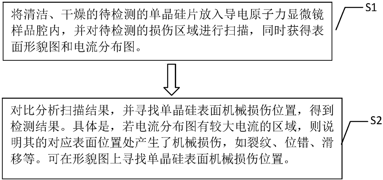
[0027] Such as figure 1 As shown, a method for detecting mechanical damage on the surface of single crystal silicon based on conductivity change, comprising the following steps:

[0028] S1. Put the clean and dry single crystal silicon wafer to be tested into the sample cavity of the conductive atomic force microscope, scan the surface damage area to be tested, and obtain the surface topography and current distribution map at the same time.

[0029] The surface of single crystal silicon is scratched with a diamond tip to obtain mechanical scratches. In this embodiment, the radius of curvature of the diamond tip is 10 μm, the load is 5 mN-20 mN, and the number of cycles is 1. After the scribing is completed, put the monocrystalline silicon wafer in absolute ethanol and acetone and clean it ultrasonically for three minutes, rinse and dry it with deionized water, and put the cleaned and dried monocrystalline silicon wafer into the conductive atomic force microscope. Inside the ...

Embodiment 2

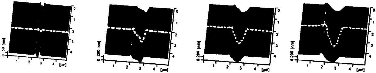
[0035] Such as figure 1 As shown, a method for detecting mechanical damage on the surface of single crystal silicon based on conductivity change, comprising the following steps:

[0036] S1. Put the clean and dry single crystal silicon wafer to be tested into the sample cavity of the conductive atomic force microscope, scan the surface damage area to be tested, and obtain the surface topography and current distribution map at the same time.

[0037] The single crystal silicon wafer with a non-destructive groove structure on the surface to be tested is placed in absolute ethanol and acetone, ultrasonically cleaned for three minutes, rinsed with deionized water and dried. Put the single crystal silicon wafer after the cleaning and drying steps into the sample cavity of the conductive atomic force microscope, and scan the damaged area to be detected.

[0038] In order to prevent the anodic oxidation reaction and displacement current on the surface of the single crystal silicon w...

Embodiment 3

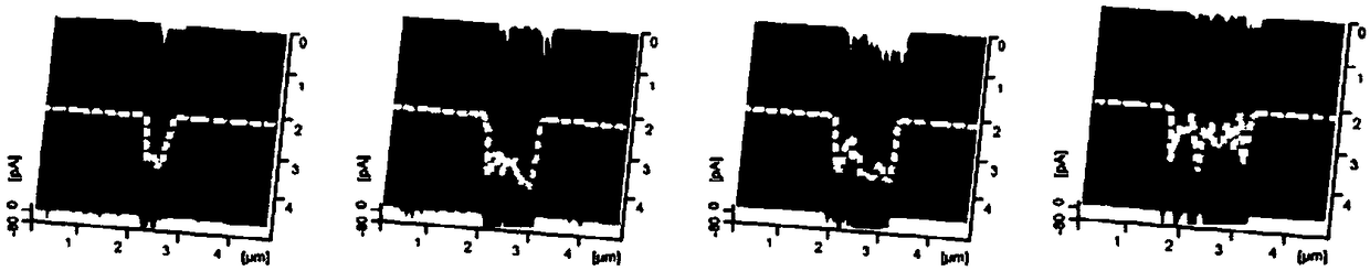
[0042] Such as figure 1 As shown, a method for detecting mechanical damage on the surface of single crystal silicon based on conductivity change, comprising the following steps:

[0043] S1. Put the clean and dry single crystal silicon wafer to be tested into the sample cavity of the conductive atomic force microscope, scan the surface damage area to be tested, and obtain the surface topography and current distribution map at the same time.

[0044]The single crystal silicon wafer was polished on a polishing machine for 10 minutes, the polishing particles used in the polishing machine were silicon carbide, and the rotational speed of the polishing machine was set at 100 r / min. The polished silicon wafers were removed and placed in absolute ethanol and acetone in sequence, ultrasonically cleaned for three minutes, rinsed with deionized water and dried. Put the single crystal silicon wafer after the cleaning and drying steps into the sample cavity of the conductive atomic force...


PUM


Abstract

The invention discloses a single-crystal-silicon surface mechanical damage detecting method based on conductivity variation. The method includes the following steps of placing a clean and dry to-be-detected single-crystal-silicon wafer into a conductive atomic power microscope sample cavity, scanning a to-be-detected damage area to obtain a surface topography and a current distribution diagram, comparing and analyzing a scanning result, and finding the position of the single-crystal-silicon surface mechanical damage to obtain the detection result. In the method, scanning and detecting are conducted by means of a micro tip of an atomic power microscope, the contact pressure is far smaller than the clinical contact pressure of single crystal silicon during yielding, and a sample can not be damaged. The method is suitable for detecting the mechanical damage generated in the cutting, grinding, polishing and other machining processes of single-crystal-silicon surfaces.

Description

technical field [0001] The invention belongs to the technical field of single crystal silicon, and in particular relates to a detection method for mechanical damage on the surface of single crystal silicon based on conductivity change. Background technique [0002] Single crystal silicon is widely used in the manufacture of semiconductor devices and integrated circuits due to its excellent mechanical and electronic properties. The surface quality of monocrystalline silicon directly affects the performance and life of the manufactured devices. Therefore, it is particularly important to detect surface damage in the production process of single crystal silicon. [0003] The nano-scale damage of single crystal silicon is mainly caused by contact processing methods such as cutting and polishing. At present, the commonly used detection methods mainly include transmission electron microscopy (TEM), X-ray diffraction and micro-Raman spectroscopy. The sample preparation process of ...

Claims


Application Information

Patent Timeline
IPC IPC(8): G01Q60/24
CPCG01Q60/24
Inventor 余丙军刘潇枭陈磊钱林茂邹乙稼周超
Owner SOUTHWEST JIAOTONG UNIV
Why Eureka
Try Eureka