Low-dimensional nano photodetector based on in-plane asymmetric local field control and preparation method thereof

A photodetector, low-dimensional nanotechnology, applied in circuits, electrical components, semiconductor devices, etc., can solve problems such as affecting the photodetection performance of the device and reducing the response speed of the device, and achieve continuous photoconductivity, responsivity and detection rate. The effect of stabilization, improved signal-to-noise ratio and response speed

Inactive Publication Date: 2018-08-14
SHANGHAI INST OF TECHNICAL PHYSICS - CHINESE ACAD OF SCI
View PDF2 Cites 6 Cited by
  • Summary
  • Abstract
  • Description
  • Claims
  • Application Information

AI Technical Summary

Problems solved by technology

[0003] However, ZnO-based photodetectors have a high intrinsic carrier concentration due to their abundant surface states and lattice defects, so there is a persistent photo

Method used


Image

  • Low-dimensional nano photodetector based on in-plane asymmetric local field control and preparation method thereof
  • Low-dimensional nano photodetector based on in-plane asymmetric local field control and preparation method thereof
  • Low-dimensional nano photodetector based on in-plane asymmetric local field control and preparation method thereof

Examples


Embodiment Construction

[0025] The specific embodiment of the present invention is described in detail below in conjunction with accompanying drawing:

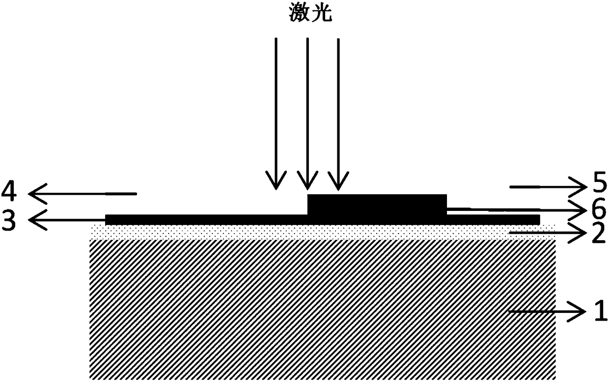
[0026] The invention develops a photodetector controlled by an in-plane asymmetric local field. Half of the ZnO channel is covered with a thin layer of HfO 2 , using the introduction of asymmetric hafnium dioxide to form a partial adsorption of charged gas molecules on the nanosheets to regulate the concentration of carriers on both sides of the ZnO nanosheets, form an in-plane asymmetric local field, and greatly improve the response time of the ZnO photodetector , with higher rectification ratio, higher detection rate and response rate.

[0027] Specific steps are as follows:

[0028] 1. Substrate Selection

[0029] Use heavily doped p-type silicon as the substrate with a resistivity of 0.05Ω cm, SiO 2 The oxide layer thickness is 300nm;

[0030] 2. Mark mark production

[0031] Use ultraviolet lithography to prepare mark patterns on p-type si...


PUM

PropertyMeasurementUnit
Thicknessaaaaaaaaaa
Length and widthaaaaaaaaaa
Thicknessaaaaaaaaaa

Abstract

The invention discloses a low-dimensional nano photodetector based on in-plane asymmetric local field control and a preparation method thereof. The device structure sequentially includes a substrate,an oxide layer, a nano semiconductor, source and drain electrodes and a dielectric layer from bottom to top. The preparation steps of the device are as follows: transferring ultra-thin zinc oxide (ZnO) nanosheets grown by using a CVD method onto a silicon substrate with the oxide layer, preparing the source and drain electrodes by using electron beam exposure, thermal evaporation and other processes, and then preparing a hafnium dioxide (HfO2) dielectric layer by using electron beam exposure, atomic layer deposition and other processes, and finally preparing a low-dimensional nano photodetector. By introducing asymmetric HfO2, the partial adsorption of charged gas molecules on the nanosheets is formed to control the concentration of carriers on both sides of the zinc oxide nanosheets, andthus an in-plane asymmetric local field is formed, the response speed of the device can be finally increased, and the device can also show an ultra-high detection rate. The scheme of the invention hasthe advantages of simple preparation, fast response speed, low dark current, high detection rate and low power consumption.

Description

technical field [0001] The invention relates to a low-dimensional nano photodetector device, in particular to a low-dimensional nano photodetector controlled by an in-plane asymmetric local field and a preparation method thereof. Background technique [0002] Due to their unique optical, electrical, magnetic and mechanical properties, two-dimensional nanostructured materials have gradually become the focus of researchers around the world in many fields such as nanodevices and functional materials. Regarding the study of low-dimensional nanostructure materials, whether it is the controllable synthesis of materials, the preparation of devices, or the study of low-dimensional physics directly related to size, there are still many problems to be solved in each link. Among them, zinc oxide (ZnO) is a typical two-dimensional material, a typical wide bandgap (3.7eV) semiconductor material, which has relatively special photoelectric conversion properties, and is also called the thir...

Claims


Application Information

Patent Timeline
IPC IPC(8): H01L31/113H01L31/0216H01L31/18
CPCH01L31/02161H01L31/1136H01L31/1836H01L31/1896Y02P70/50
Inventor 胡伟达汪洋龙明生王现英王鹏陈效双陆卫
Owner SHANGHAI INST OF TECHNICAL PHYSICS - CHINESE ACAD OF SCI
Why Eureka
Try Eureka