Preparation method of epitaxial wafer for 8-inch high-power IGBT component

A technology for components and epitaxial wafers, which is used in semiconductor/solid-state device manufacturing, electrical components, semiconductor devices, etc., can solve the problems of high output efficiency, low efficiency, and increased splintering rate, so as to avoid the increase of splintering rate and improve the Growth rate, the effect of improving electrical parameters

Active Publication Date: 2018-08-17
NANJING GUOSHENG ELECTRONICS
View PDF6 Cites 5 Cited by
  • Summary
  • Abstract
  • Description
  • Claims
  • Application Information

AI Technical Summary

Problems solved by technology

In the field of epitaxial technology, if the growth rate is fast, the output efficiency will be high; otherwise, the efficiency will be low
However, for the epitaxial wafers for 8-inch high-power IGBT components, due to the thicker growth thickness, simply increasing the growth rate will lead to a substantial increase in the split rate during the epitaxy process; growth temperature, but then introduces the problem of slip lines

Method used


Image

  • Preparation method of epitaxial wafer for 8-inch high-power IGBT component
  • Preparation method of epitaxial wafer for 8-inch high-power IGBT component

Examples


preparation example Construction

[0021] A kind of preparation method of the epitaxial wafer for 8-inch high-power IGBT component of the present invention comprises the following steps:

[0022] A. Preparing the substrate sheet: select an 8-inch substrate sheet doped with phosphorus, with a resistivity of 3-25Ω·cm, and the back-sealing structure is polycrystalline (Poly) back-sealing mode;

[0023] B. Reactor cleaning: The quartz bell jar and quartz support must be carefully cleaned before high-resistance epitaxy to remove impurity atoms and residues adsorbed on the inner wall of the quartz reactor and quartz parts;

[0024] C. Graphite pedestal treatment: before growing epitaxy, the remaining silicon and impurities on the surface of the pedestal are treated with HCl gas;

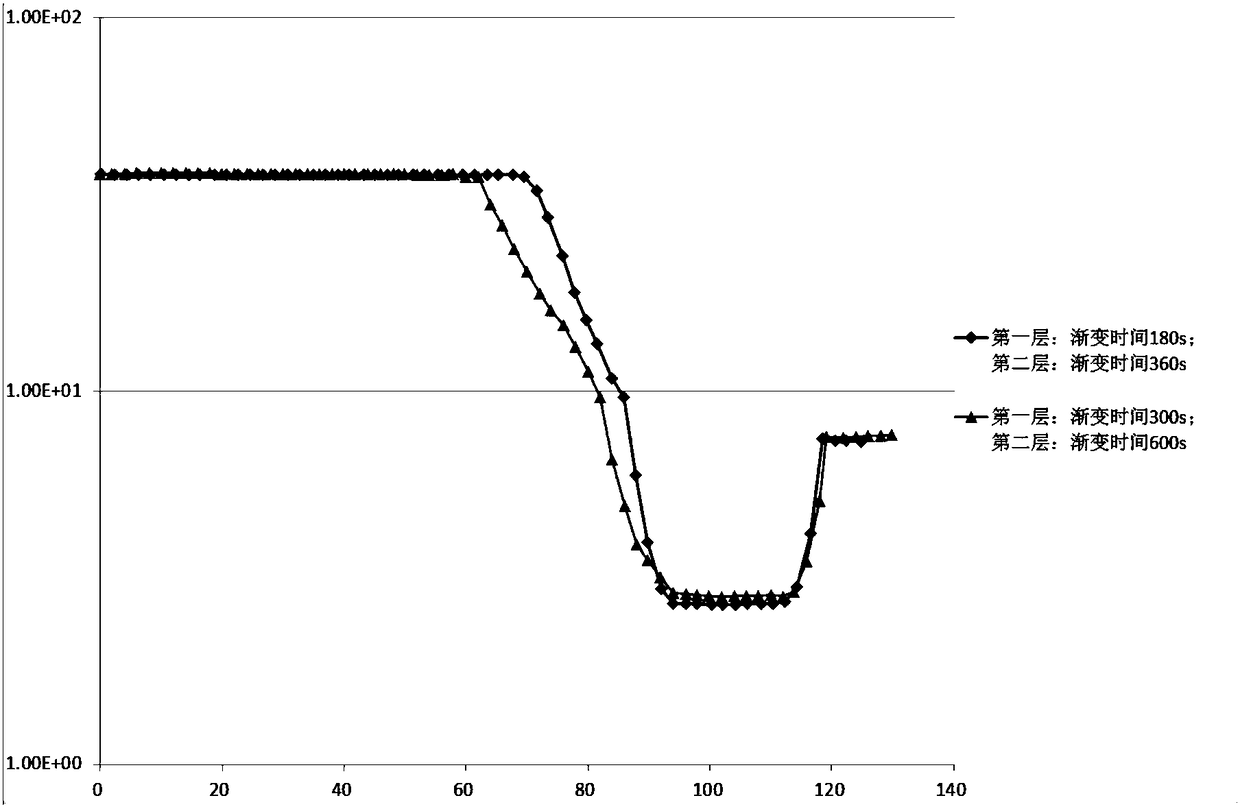
[0025] D. Epitaxial vapor phase etching: HCl polishing, at 1080°C, select the HCl flow rate to be 1-2L / min, the polishing time is 2min, and the large flow rate of H after polishing is completed. 2 Purge for 3 minutes; the purpose of vapor ...

Embodiment 1

[0028] A kind of preparation method of the epitaxial wafer for 8-inch high-power IGBT component of the present invention comprises the following steps:

[0029] A. Preparing the substrate sheet: select an 8-inch substrate sheet doped with phosphorus, with a resistivity of 3-25Ω·cm, and the back-sealing structure is polycrystalline (Poly) back-sealing mode;

[0030] B. Reactor cleaning: The quartz bell jar and quartz support must be carefully cleaned before high-resistance epitaxy to remove impurity atoms and residues adsorbed on the inner wall of the quartz reactor and quartz parts;

[0031] C. Graphite pedestal treatment: before growing epitaxy, the pedestal must be reprocessed;

[0032] D. Epitaxial vapor phase etching: HCl polishing, at 1080°C, select the HCl flow rate as 1L / min, the polishing time is 2min, and the large flow rate of H after the polishing is completed. 2 Purge for 3 minutes; the purpose of vapor phase corrosion is to remove the natural oxide layer on the s...

Embodiment 2

[0035] A kind of preparation method of the epitaxial wafer for 8-inch high-power IGBT component of the present invention comprises the following steps:

[0036] A. Preparing the substrate sheet: select an 8-inch substrate sheet doped with phosphorus, with a resistivity of 3-25Ω·cm, and the back-sealing structure is polycrystalline (Poly) back-sealing mode;

[0037] B. Reactor cleaning: The quartz bell jar and quartz support must be carefully cleaned before high-resistance epitaxy to remove impurity atoms and residues adsorbed on the inner wall of the quartz reactor and quartz parts;

[0038] C. Graphite pedestal treatment: before growing epitaxy, the pedestal must be reprocessed;

[0039] D. Epitaxial vapor phase etching: HCl polishing, at 1080°C, select the HCl flow rate as 1L / min, the polishing time is 2min, and the large flow rate of H after the polishing is completed. 2 Purge for 3 minutes; the purpose of vapor phase corrosion is to remove the natural oxide layer on the s...


PUM


Abstract

The invention discloses a preparation method of an epitaxial wafer for an 8-inch high-power IGBT component. The method includes following steps: preparing a substrate: selecting an 8-inch substrate with a p-doped middle resistance, wherein the resistivity is 3-25 ohm*cm, and a back-sealing structure is in a polycrystalline (Poly) back-sealing mode; HCl polishing: selecting the HCl flow of 1-2 L/min at the temperature lower than 1080 DEG C with the polishing time of 2 minutes, and performing purging with high-flow H2 for 3 minutes after completion of polishing; and epitaxial growth: selecting at least three layers of epitaxial process conditions, wherein a silicon source employs ultra-high-purity trichlorosilane, the epitaxial growth of each layer employs the same growth temperature and growth rate, an epitaxial layer with flat resistivity is grown on a first layer, an intermediate transition layer is grown on an intermediate layer through introduction of a doping source with a variabledoping flow, and a high-resistance epitaxial layer is grown on a final layer. According to the method, the growth of the epitaxial layer of each layer employs the same growth rate and growth temperature so that the controllability of epitaxial parameters of products in a batch production process is facilitated.

Description

technical field [0001] The invention relates to a silicon epitaxial wafer, a basic semiconductor material, in particular to a preparation method for an 8-inch high-power IGBT component epitaxial wafer. Background technique [0002] The epitaxial growth process is a method of depositing a thin layer of a single crystal on the surface of a single crystal substrate. Vapor phase epitaxy is the most widely used due to the good control of impurity concentration and the ability to obtain crystal integrity. [0003] Insulated gate bipolar transistor (IGBT for short) is a new type of composite power device developed on the basis of metal oxide field effect transistors and bipolar transistors, with MOS input and bipolar output functions. IGBT combines the advantages of small on-state voltage drop of bipolar transistor devices, high current carrying density, high withstand voltage, low driving power of metal oxide field effect transistors, fast switching speed, high input impedance, a...

Claims


Application Information

Patent Timeline
Patent Type & Authority Applications(China)
IPC IPC(8): H01L21/02H01L29/16H01L29/739
CPCH01L21/02013H01L21/02532H01L21/02634H01L29/16H01L29/7393
Inventor 魏建宇骆红葛华
Owner NANJING GUOSHENG ELECTRONICS
Why Eureka
Try Eureka