Preparation method of wafer level graphene micro-nano monocrystal array

A graphene, micro-nano technology, applied in the direction of single crystal growth, single crystal growth, chemical instruments and methods, etc., can solve the problems of inability to prepare large areas, complicated steps of graphene micro-nano single crystal array, etc., and achieve good application prospects , the effect of less defects and controllable size

Inactive Publication Date: 2018-08-24
HUAZHONG UNIV OF SCI & TECH
View PDF2 Cites 7 Cited by
  • Summary
  • Abstract
  • Description
  • Claims
  • Application Information

AI Technical Summary

Problems solved by technology

[0004] In view of the above defects or improvement needs of the prior art, the present invention provides a method for preparing a wafer-level graphene micro-nano single crystal array, the purpose of which is to realize the one-step vapor deposition process by controlling the atmosphere in the chemical vapor deposition process. method, naturally formed large-area such as wafer-level graphene micro-nano single-crystal array preparation method, thereby solving the technical problems of the prior art for preparing graphene micro-nano single-crystal arrays with complex steps and incapable of large-scale preparation.

Method used


Image

  • Preparation method of wafer level graphene micro-nano monocrystal array
  • Preparation method of wafer level graphene micro-nano monocrystal array
  • Preparation method of wafer level graphene micro-nano monocrystal array

Examples


preparation example Construction

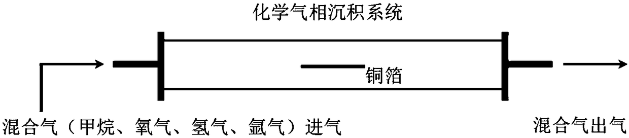
[0030] The method for preparing a graphene micro / nano single crystal array provided by the present invention may specifically include the following steps:

[0031] (1) Pretreatment of copper foil: After immersing the copper foil in a 1:1:1 mixed solution of acetic acid, ethanol and deionized water for 15 minutes, rinse it with deionized water, and then dry it with nitrogen; Commercially available single crystal copper foil or polycrystalline copper foil can be used as the copper foil.

[0032] (2) The temperature rise of the metal copper foil: Put the cleaned and dry copper foil in a chemical vapor deposition system, and pass in argon gas. The temperature will rise to 1000-1030°C within 30-60 minutes, and then pass in hydrogen gas to make hydrogen The volume fraction of the mixed gas in the system is 1.8-2.1%, and the temperature is continued to rise to 1050-1070°C, and the temperature range is maintained for 10-30 minutes.

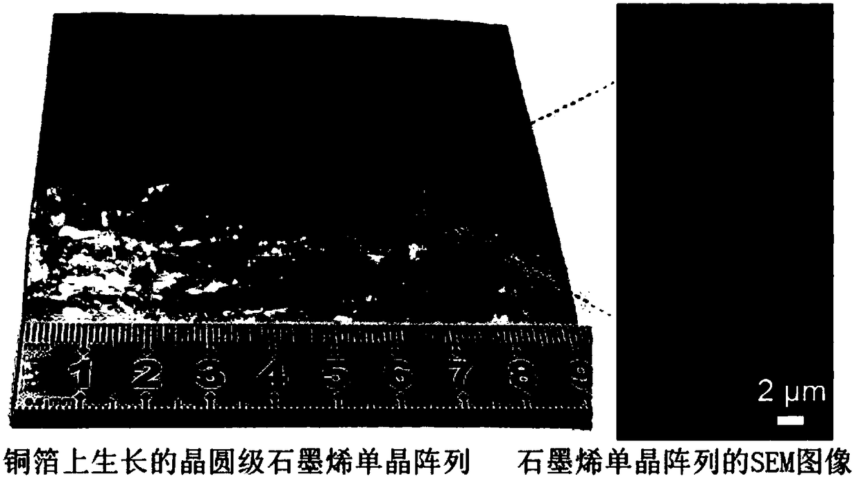
[0033] (3) Direct growth of graphene single crystal array...

Embodiment 2

[0045] (1) The size of 3 pieces is 9*9cm 2 Copper foil with a size and thickness of 100 microns is soaked in a 1:1:1 mixed solution of acetic acid, ethanol and deionized water for 15 minutes, rinsed with deionized water, and dried with nitrogen.

[0046] (2) Put the cleaned 3 pieces of copper foil into the chemical vapor deposition system, and pass in 500sccm argon to remove the clean air. The temperature will be raised to 1030℃ within 40 minutes, and then the high purity hydrogen at a flow rate of 10sccm will be introduced, and the temperature will continue to rise to 1070°C and keep the temperature constant for 10 minutes.

[0047] (3) Keep the temperature and the flow of argon and hydrogen unchanged, continue to feed 5 sccm of methane with a concentration of 2% into the chemical vapor deposition system, and feed 2-4 sccm of oxygen with a concentration of 0.1% respectively, under normal pressure conditions After 5 hours of growth, the temperature is lowered to room temperature, e...


PUM

PropertyMeasurementUnit
volume ratioaaaaaaaaaa

Abstract

The invention belongs to the technical field of graphene material synthesis and preparation and more particularly relates to a preparation method of a wafer level graphene micro-nano monocrystal array. The method comprises the steps of performing chemical vapor deposition on the surface of polycrystal copper foil in a mixed atmosphere containing methane and oxygen for growth to form the graphene micro-nano monocrystal array, wherein methane serves as a carbon source for graphene growth; the copper foil serves as a catalytical substrate for the graphene growth; and the oxygen serves as etchinggas in a formation process of the graphene monocrystal array. According to the method, a graphene array structure is directly prepared by a simple one-step chemical vapor deposition method; the disadvantage of complicated steps of complicated micro-nano machining, etching and the like required by a graphene film in a subsequent application is overcome; quick and low-cost preparation of a large area micro-nano graphene monocrystal is achieved; and the application in large-scale device preparation is facilitated.

Description

Technical field [0001] The invention belongs to the technical field of graphene material synthesis and preparation, and more specifically relates to a method for preparing a wafer-level graphene micro-nano single crystal array. Background technique [0002] Since the single-layer graphene was first peeled off in 2004, related research has reached unprecedented heights. Its excellent photoelectric, mechanical, and chemical properties make it a promising functional material. At present, chemical vapor deposition is the most effective method for large-scale preparation of single-layer high-quality graphene, resulting in a continuous film. Generally speaking, to realize the practical application of graphene in devices, it is necessary to process graphene into a specific integrated structure of micro-nano scale. These steps often rely on artificially designed micro-nano processing and etching technologies, which will bring many tedious post-processing steps, which will increase the c...

Claims


Application Information

Patent Timeline
Patent Type & Authority Applications(China)
IPC IPC(8): C30B29/02C30B25/16
CPCC30B25/165C30B29/02
Inventor 王帅郭巍池凯
Owner HUAZHONG UNIV OF SCI & TECH
Why Eureka
Try Eureka