UV-infrared double-wave band integrated p-i-n type photoelectric detector

A p-i-n, photodetector technology, applied in the direction of circuits, electrical components, semiconductor devices, etc., can solve the problems of complex optical system and device preparation process, increasing the difficulty of growing heterogeneous materials, etc.

Pending Publication Date: 2018-08-31
XIAMEN UNIV
View PDF1 Cites 4 Cited by
  • Summary
  • Abstract
  • Description
  • Claims
  • Application Information

AI Technical Summary

Problems solved by technology

[0004] However, most current ultraviolet-infrared dual-band detectors are mainly composed of two detection components that respond to different wavebands respectively. The method of installing interco

Method used


Image

  • UV-infrared double-wave band integrated p-i-n type photoelectric detector
  • UV-infrared double-wave band integrated p-i-n type photoelectric detector
  • UV-infrared double-wave band integrated p-i-n type photoelectric detector

Examples


Embodiment 1

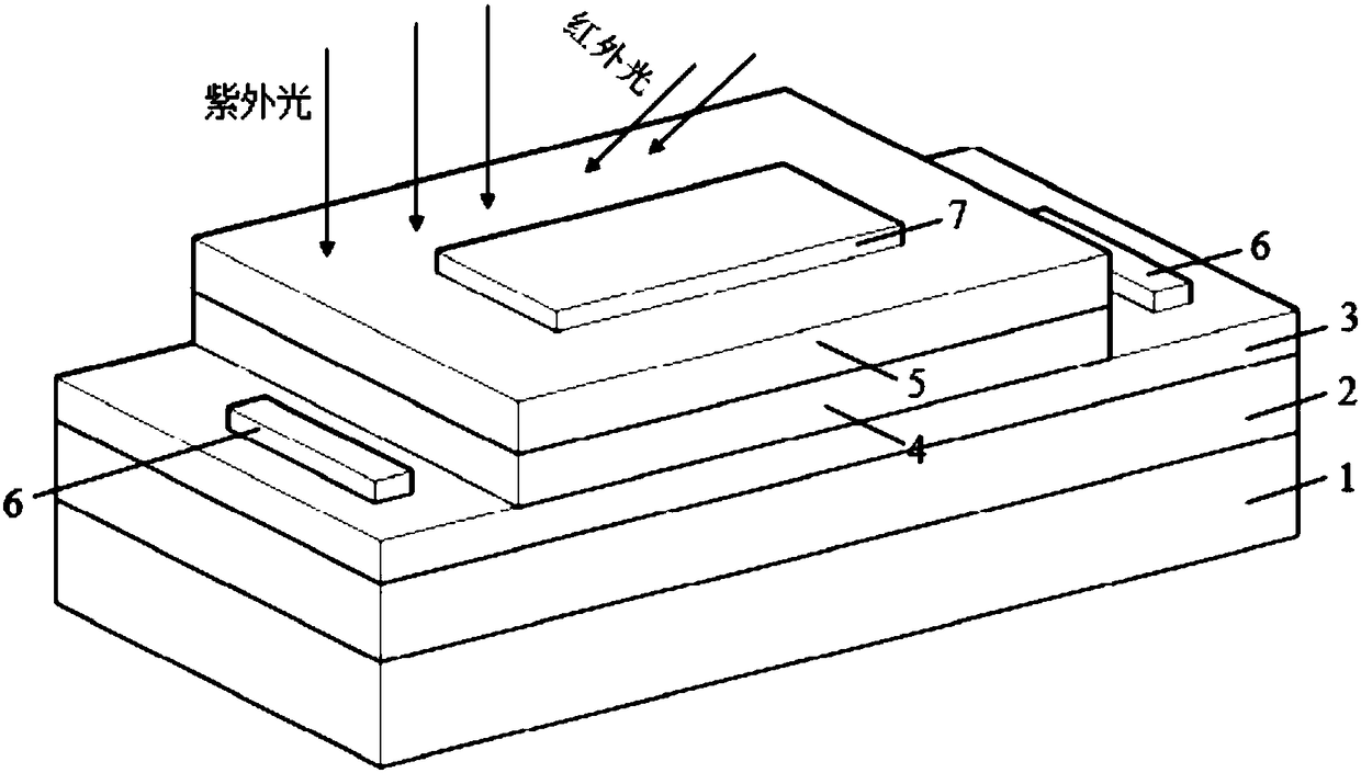
[0037] The fabrication method of the above-mentioned ultraviolet-infrared dual-band integrated p-i-n photodetector is as follows:

[0038] i) growing an AlN buffer layer 2 with a thickness of about 100 nm to 1 μm on the c-surface of the sapphire substrate by metal-organic vapor phase epitaxy;

[0039]ii) growing n-type ultra-short-period superlattice 3 , non-doped i-type ultra-short-period superlattice 4 , and p-type ultra-short-period superlattice 5 sequentially on the above-mentioned AlN buffer layer 2 . In the actual growth process, trimethylgallium (TMG) and trimethylaluminum (TMA) were used as group III sources, ammonia (NH 3 ) as the V group source, while using dipentyl magnesium (Cp 2 Mg) and silane (SiH 4 ) as p-type and n-type impurity sources, hydrogen (H 2 ) as the carrier gas.

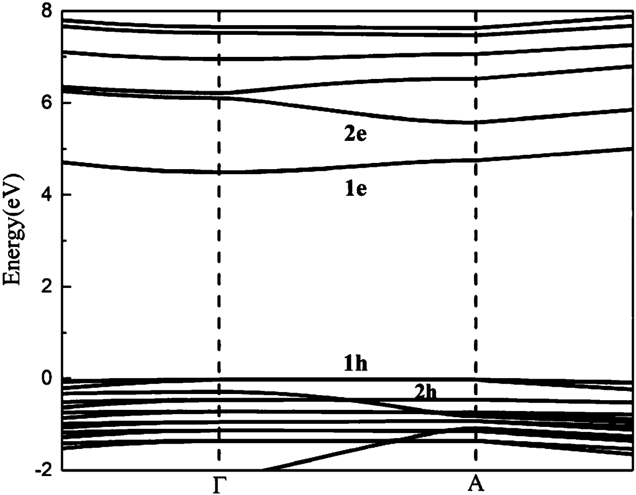
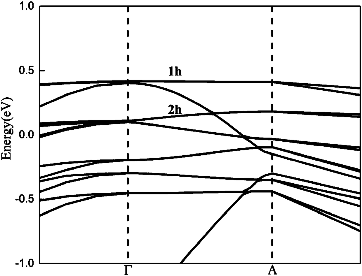
[0040] The non-doped i-type ultra-short-period superlattice 4 adopts a GaN / AlN ultra-short-period supercrystalline structure, and uses growth interruption technology to control the GaN ...

Embodiment 2

[0049] In this embodiment, the layered structure of the ultraviolet-infrared dual-band integrated p-i-n photodetector is the same as that of embodiment 1, and the specific manufacturing steps are as follows:

[0050] i) Using metal-organic vapor phase epitaxy, sequentially grow AlN buffer layer 2, n-type ultra-short period superlattice 3, non-doped i-type ultra-short period superlattice 4, p-type ultrashort period superlattice Periodic superlattice 5. The epitaxy steps are the same as those in Embodiment 1.

[0051] ii) Grinding the side of the above-mentioned complete p-i-n epitaxial structure facing the side of the substrate 1 and making it form an angle of 45°, so as to satisfy the polarization selection condition of the sub-band transition.

[0052] iii) Similarly, use standard photolithography, ICP etching and electron beam deposition and other micromachining processes to etch n-type mesas and deposit titanium / aluminum / titanium / gold alloys on them, and form n-type ultras...


PUM

PropertyMeasurementUnit
Doping concentrationaaaaaaaaaa

Abstract

The invention provides an UV-infrared double-wave band integrated p-i-n type photoelectric detector comprising a substrate, a buffer layer, a n-type ultra short period superlattice, a non-doped i typeultra short period superlattice, and a p type ultra short period superlattice stacked from bottom to top; the n type ultra short period superlattice has an exposed area on the side face of the non-doped i type ultra short period superlattice; a n type ohmic contact electrode is arranged on the top surface of the exposed area, and a p type ohmic contact electrode is arranged on the top surface ofthe p type ultra short period superlattice; the non-doped i type ultra short period superlattice can satisfy luminous absorption transition of carriers between valence band and conduction band quantumenergy levels, or ultraviolet irradiation and infrared light incident modes can cooperate so as to enable in-valence band carriers to absorb photons and make in-band inter-quantum energy level transition, thus realizing UV-infrared double-wave band optical signal detection identification; the infrared wave band optical signal can change the doped concentration of the p type ultra short period superlattice, thus realizing response detection.

Description

technical field [0001] The invention belongs to the technical field of semiconductor optoelectronic devices, in particular to an ultraviolet-infrared dual-band integrated p-i-n photodetector. Background technique [0002] In recent years, with the improvement of the quality of third-generation wide-bandgap semiconductor materials and the maturity of key device processes, ultraviolet and even deep ultraviolet photodetectors have gradually emerged in the modern military arena and civilian life. Among them, the photodetector whose operating wavelength is in the deep ultraviolet region takes advantage of the extremely limited or even weak solar radiation energy in the solar blind area, and can distinguish and identify the target ultraviolet radiation signal in a natural low-noise background. It has broad application prospects in the fields of missile plume component detection, aerospace tracking and control, biomedical engineering analysis, and ultraviolet high-security communic...

Claims


Application Information

Patent Timeline
IPC IPC(8): H01L31/105
CPCH01L31/105
Inventor 高娜冯向黄凯葛树成李书平康俊勇
Owner XIAMEN UNIV
Why Eureka
Try Eureka