Crucible for silicon carbide single crystal growing close to equilibrium state and growing method of silicon carbide single crystal

An equilibrium state, crucible technology, applied in the direction of single crystal growth, single crystal growth, crystal growth, etc., can solve the problems of device performance stability, reliability, structural defects, influence, etc., and achieve low single crystal stress, high quality, and defect density. low effect

Inactive Publication Date: 2018-09-28
SHANDONG UNIV
View PDF0 Cites 14 Cited by
  • Summary
  • Abstract
  • Description
  • Claims
  • Application Information

AI Technical Summary

Problems solved by technology

[0004] At present, SiC single crystal substrates have been used to prepare semiconductor devices such as high-power semiconductor lighting LEDs, high electron mobility transistors, Schottky diodes, metal oxide semiconductor field effect transistors, etc., but the performance stability and long-term reliability of the devices properties are still affected by structural defects in the substrate material
How to reduce structural defects in SiC single crystals and obtain SiC single crystals with high structural integrity is a serious challenge for crystal growth work, and it is also a long-term and arduous research topic

Method used


Image

  • Crucible for silicon carbide single crystal growing close to equilibrium state and growing method of silicon carbide single crystal
  • Crucible for silicon carbide single crystal growing close to equilibrium state and growing method of silicon carbide single crystal

Examples


Embodiment 1

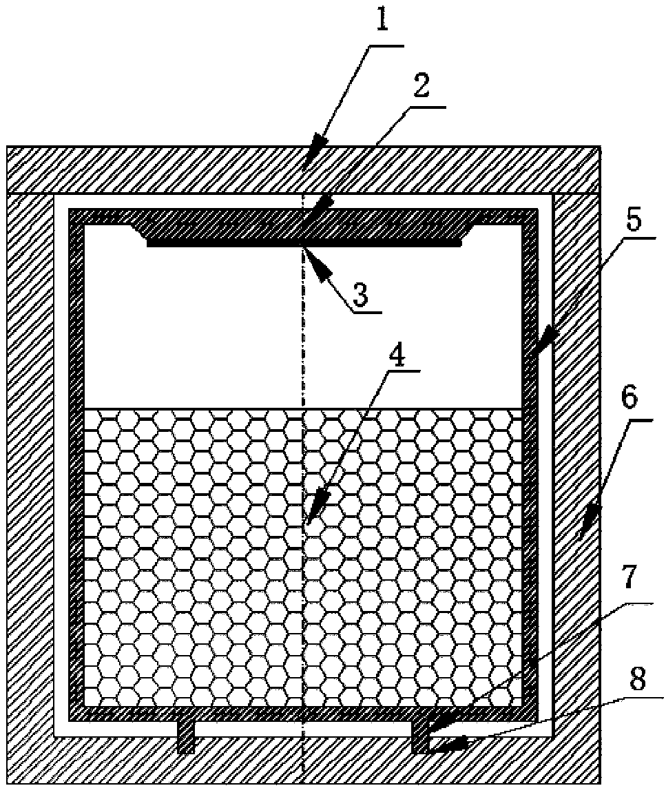
[0041] A crucible for growing near-equilibrium SiC single crystals, the structure is as follows figure 1 As shown, it includes an outer crucible and an inner crucible, the outer crucible is a heating body, the inner crucible is a growth crucible, and there is a distance between the outer crucible and the inner crucible, and the distance is 6mm;

[0042] The outer crucible includes an outer crucible body 6 and an outer crucible cover 1, both of which are made of graphite, wherein the upper end of the outer crucible body 6 is evenly distributed with 4 screw holes, the outer crucible cover 1 is evenly distributed with 4 through holes correspondingly, and the graphite screws pass through. Screw holes and through holes seal the outer crucible body 6 with the outer crucible cover 1;

[0043] Wherein, the outer crucible body 6 includes an outer crucible side wall and an outer crucible bottom, both of which are integral structures, the inner and outer contours are cylindrical, and the...

Embodiment 2

[0052] A kind of crucible for growing near-equilibrium SiC single crystal as described in Example 1, the difference is:

[0053] The distance between the outer crucible and the inner crucible is 8 mm, the thickness of the outer crucible body 6 and the outer crucible cover 1 is 18 mm, the thickness of the inner crucible body 5 is 7 mm, and the upper circle of the inner crucible cover 2 is round. The thickness of the shape and the thickness of the lower rounded frustum are 7mm, and the taper angle of the rounded frustum is 45°.

Embodiment 3

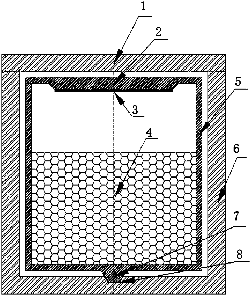
[0055] A crucible for growing near-equilibrium SiC single crystals, as shown in the schematic diagram figure 2 As shown, compared with Example 1, the difference is:

[0056] The positioning pin 7 on the outer side of the bottom of the inner crucible body 5 is not cylindrical, but a rounded truncated cone, located at the center of the outer side of the inner crucible bottom, with a large upper end diameter and a small lower end diameter. Correspondingly, the bottom inner positioning hole 8 of the outer crucible body 6 is: Rounded truncated truncated locating pin 7 with contour matching. Since the position closer to the center of the crucible, the lower the temperature, with this positioning pin, the heat transmitted by the bottom through conduction is less than that in Example 1, which is more conducive to reducing the temperature gradient in the powder in the inner crucible.


PUM

PropertyMeasurementUnit
Thicknessaaaaaaaaaa
Thicknessaaaaaaaaaa
Thicknessaaaaaaaaaa

Abstract

The invention relates to a crucible for a silicon carbide single crystal growing close to an equilibrium state and a growing method of the silicon carbide single crystal. The crucible comprises an outer crucible and an inner crucible, wherein the outer crucible is a heating element, and the inner crucible is a growing crucible; the separation distance between the outer crucible and the inner crucible is 5-10 millimeters. The provided crucible for the silicon carbide single crystal growing close to the equilibrium state has the advantages that the heating element and the growing crucible are separated, the outer crucible plays a role of the heating element, the inner crucible is the growing crucible, the heat of the outer crucible is transmitted into the inner crucible mainly through a radiation method, the inner crucible has the characteristics of small radial and axial temperature gradients, a novel crucible is adopted, the growth of the single crystal is performed under a condition close to the equilibrium state, so that the defect density of the grown single crystal is low, and the crucible is suitable for culturing a high-quality silicon carbide single crystal.

Description

technical field [0001] The invention relates to a crucible for growing a near-equilibrium SiC single crystal and a growth method of the SiC single crystal, belonging to the technical field of crystal growth. Background technique [0002] Silicon carbide (SiC) semiconductor, also known as wide bandgap semiconductor or third-generation semiconductor, has high hardness (second only to diamond) and high thermal conductivity (4.9 compared with the first-generation semiconductor Si and the second-generation semiconductor GaAs). W / cm·K), low thermal expansion coefficient (3.1-4.5×10 -6 / K), large forbidden band width (2.40-3.26eV), high saturation electron drift velocity (2.0-2.5×10 7 cm / s), the critical breakdown field is strong (2~3×10 6 V / cm), high chemical stability, strong radiation resistance and other excellent properties. These excellent properties enable SiC semiconductor devices to work in extreme environments of high temperature, high pressure, and strong radiation, a...

Claims


Application Information

Patent Timeline
IPC IPC(8): C30B23/06C30B29/36
CPCC30B23/066C30B29/36
Inventor 胡小波徐现刚陈秀芳彭燕杨祥龙
Owner SHANDONG UNIV
Why Eureka
Try Eureka