Photocatalyst, photocatalyst film and their preparation methods and application
A photocatalyst and thin film technology, applied in the field of photocatalytic reaction, can solve the problems of reducing charge separation and photocatalytic performance, and achieve the effect of enhancing photocatalytic efficiency and improving photocatalytic sterilization efficiency
- Summary
- Abstract
- Description
- Claims
- Application Information
AI Technical Summary
Problems solved by technology
Method used
Image

Examples
preparation example Construction
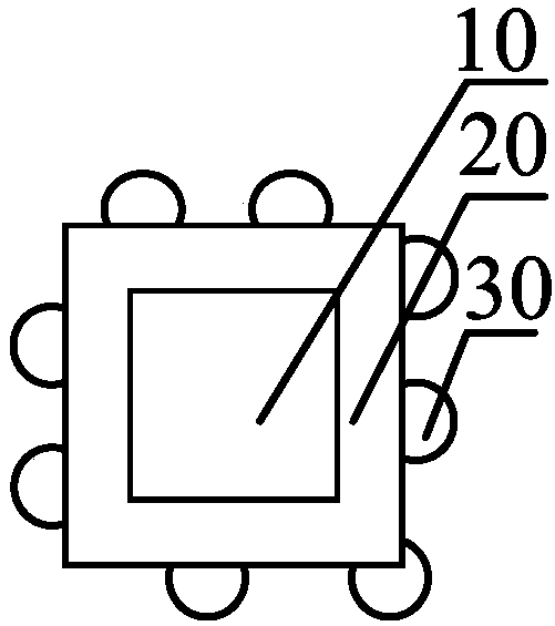
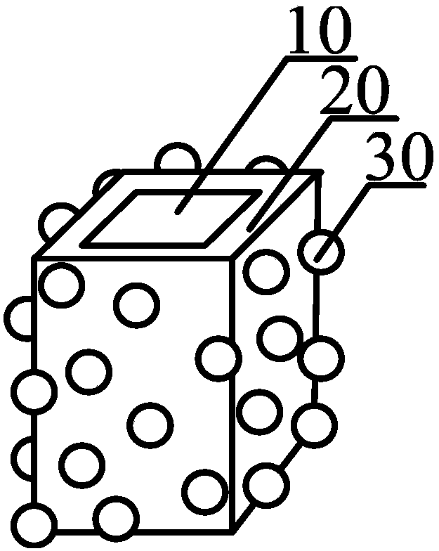
[0039] According to the third aspect of the present invention, there is also provided a method for preparing the above-mentioned photocatalyst according to the present invention. The preparation method includes: S1, providing a core including a first semiconductor material; S2, on the outer periphery of the core Coating and forming an intermediate layer including piezoelectric material to obtain an intermediate; S3, forming an outer layer including a second semiconductor material and / or metal nanoparticles with surface plasmon effect on the periphery of the intermediate to obtain a photocatalyst, The second semiconductor material and the first semiconductor material are the same or different.
[0040] According to the above preparation method of the present invention, preferably, the core of S1 is a nanowire, nanotube or nano-scale film; preferably, the core of S1 is a nanowire or nanotube, and more preferably, the S1 is electrically conductive. The nanowire array or nanotube arr...
Embodiment 1
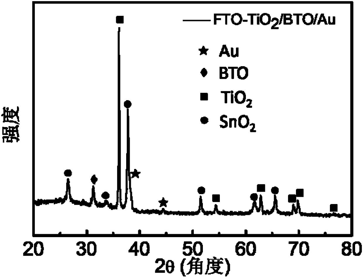
[0086] Preparation of TiO 2 / BaTiO 3 / Au photocatalyst film
[0087] The method for preparing the photocatalyst film includes the following steps:
[0088] (1) Grow TiO on conductive glass substrate 2 Nanowire array: Add 2ml of tetrabutyl titanate (commercially purchased from Beijing Chemical Plant, analytically pure) into a mixed solution of 20ml deionized water and 20ml concentrated hydrochloric acid (mass fraction 37%) and stir evenly to obtain H + It is a 6mol / L acid mixture. Put the acid mixture into a 50ml reaction kettle, and then put the cleaned conductive glass substrate (commercially purchased from Zhuhai Kaiwei Photoelectric Co., Ltd. doped SnO 2 The conductive glass product, the size is 100×100×1.6mm, the same below) is immersed in it. The reaction kettle was sealed and put into a drying box. The reaction time at 180°C was 6h. After the reaction, it was naturally cooled to room temperature. The conductive glass substrate was taken out to clean the remaining reactants on...
Embodiment 2
[0098] Preparation of TiO 2 / PbTiO 3 / Au photocatalyst film
[0099] The method for preparing the photocatalyst film includes the following steps:
[0100] (1) TiO growth on conductive glass substrate 2 Nanowire array: same as Example 1;
[0101] (2) Form PbTiO 3 Piezoelectric material middle layer: Dissolve 2ml of tetrabutyl titanate in 20ml of ethanol, then add 5ml of 0.01mol / L lead acetate aqueous solution, stir well, and grow the prepared TiO 2 The conductive glass substrate of the nanowire array is placed in it, and it is put into the reactor for hydrothermal synthesis at 160°C for 4 hours to obtain the intermediate array (PbTiO formed on the surface of the conductive glass substrate). 3 The thickness of the piezoelectric material layer is 4-15nm);
[0102] (3) Supporting Au nanoparticle outer layer: referring to Example 1, the difference is that the intermediate array grown on the conductive glass substrate in the above step (2) is used to obtain the photocatalyst array (gold nan...
PUM
| Property | Measurement | Unit |
|---|---|---|
| diameter | aaaaa | aaaaa |
| length | aaaaa | aaaaa |
| thickness | aaaaa | aaaaa |
Abstract
Description
Claims
Application Information
 - R&D
- Intellectual Property
- Life Sciences
- Materials
- Tech Scout
- Unparalleled Data Quality
- Higher Quality Content
- 60% Fewer Hallucinations
Browse by: Latest US Patents, China's latest patents, Technical Efficacy Thesaurus, Application Domain, Technology Topic, Popular Technical Reports.
© 2025 PatSnap. All rights reserved.Legal|Privacy policy|Modern Slavery Act Transparency Statement|Sitemap|About US| Contact US: help@patsnap.com