Growth method of p-type AlGaN semiconductor material

A growth method, semiconductor technology, applied in semiconductor/solid-state device manufacturing, electrical components, circuits, etc., can solve the disadvantages of large-scale production and commercial application, can not improve the donor compensation effect, can not increase the concentration of magnesium doping, etc. problem, to achieve the effect of improving interface roughness, enhancing retention, and increasing the probability of incorporation

Active Publication Date: 2018-12-11
SUN YAT SEN UNIV
View PDF9 Cites 8 Cited by
  • Summary
  • Abstract
  • Description
  • Claims
  • Application Information

AI Technical Summary

Problems solved by technology

Although this method can make good use of the two-dimensional hole gas formed by the band bending of the heterointerface to obtain a higher hole concentration, the superlattice doping cannot increase the doping concentration of magnesium, nor can it improve the donor density. sexual compensation effect
In addition, since the superlattice structure is composed of two semiconductor materials with different bandgap widths alternately stacked and grown, it will have a negative impact on the transport of carriers, light emission or incident absorption in optoelectronic devices; the use of acceptor-donor Co-doping method (High Doped p-Type GaNGrown by Alter native Co-Doping Technique, Mat.Res.Soc.Symp.Proc.Vol.719, 2002), although it can be used by using the Coulomb interaction between the acceptor-donor To effectively reduce the ionization energy of acceptor-doped magnesium atoms, but the growth window of this method is very narrow, it is difficult to realize, and it is not conducive to large-scale production and commercial application

Method used


Image

  • Growth method of p-type AlGaN semiconductor material
  • Growth method of p-type AlGaN semiconductor material
  • Growth method of p-type AlGaN semiconductor material

Examples


Embodiment 1

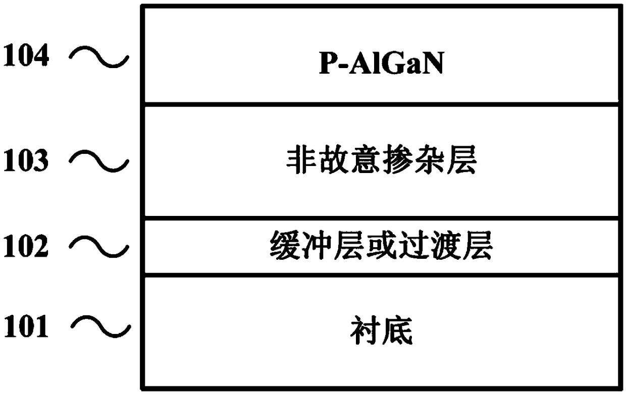
[0044] Such as image 3 As shown, the epitaxial growth structure of the p-type AlGaN semiconductor material of the present invention includes a substrate 101 , a buffer layer or transition layer 102 , an unintentionally doped layer 103 and an acceptor doped layer (p-type AlGaN semiconductor material layer) 104 . The substrate 101 is a sapphire substrate, a buffer layer 102 is grown on the substrate 101 by a metal organic chemical vapor deposition (MOCVD) epitaxial growth method, and a buffer layer 102 is grown on the buffer layer by a metal organic chemical vapor deposition (MOCVD) epitaxial growth method. The method grows an unintentionally doped AlGaN layer 103 and grows a p-type AlGaN semiconductor material layer 104 on the unintentionally doped AlGaN layer 103 by metal organic chemical vapor deposition (MOCVD) epitaxial growth method.

[0045] In the growth process of this implementation case, ammonia gas is used as the source of group V nitrogen; trimethylgallium is used ...

Embodiment 2

[0057] Such as image 3 As shown, the epitaxial growth structure of the p-type AlGaN semiconductor material of the present invention includes a substrate 101 , a buffer layer or transition layer 102 , an unintentionally doped layer 103 and an acceptor doped layer (p-type AlGaN semiconductor material layer) 104 . The substrate 101 is a silicon carbide substrate, and a buffer layer 102 is sequentially grown on the substrate 101 by a metal organic chemical vapor deposition (MOCVD) epitaxial growth method, and a metal organic chemical vapor deposition (MOCVD) epitaxy method is used on the buffer layer to grow The growth method grows the unintentionally doped AlGaN layer 103 and grows the p-type AlGaN semiconductor material layer 104 on the unintentionally doped AlGaN layer 103 by metal organic chemical vapor deposition (MOCVD) epitaxial growth method.

[0058] In the growth process of this implementation case, dimethylhydrazine nitrogen is used as the source of group V nitrogen; t...

Embodiment 3

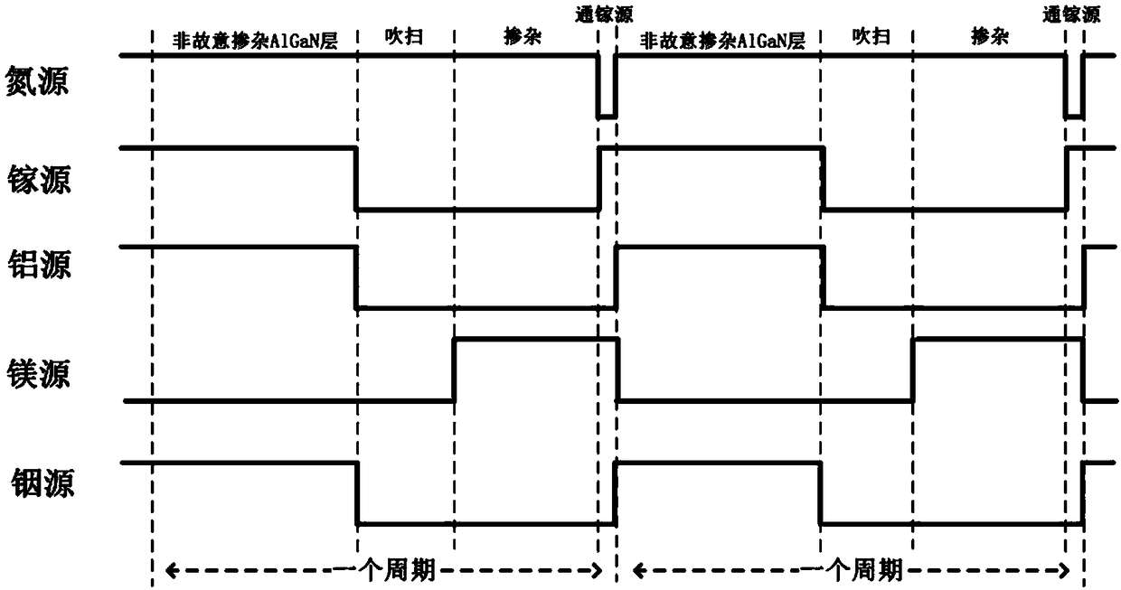
[0070] The p-type AlGaN semiconductor material in this embodiment is grown on the AlN material substrate layer with a thickness of 500nm and a growth temperature of 900°C. In the growth process of this embodiment, ammonia gas is used as the source of Group V nitrogen; Gallium-based is used as the source of Group III gallium, and trimethylaluminum is used as the source of Group III aluminum; trimethylindium is used as a surfactant, which specifically includes the following steps:

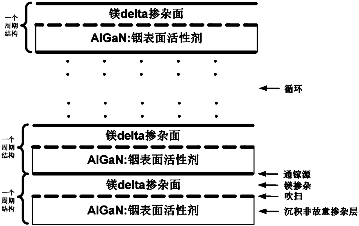
[0071] Deposition of unintentionally doped AlGaN layer: use hydrogen as the carrier gas, keep the V-group nitrogen source continuously fed, pass through the III-group gallium source, the III-group aluminum source and the triethylindium surfactant, and deposit unintentionally doped AlGaN layer;

[0072] Purge: use hydrogen as the carrier gas, keep the V-group nitrogen source continuously fed, disconnect the III-group gallium source, III-group aluminum source and surfactant for 40s, and purge the surfa...


PUM

PropertyMeasurementUnit
thicknessaaaaaaaaaa
thicknessaaaaaaaaaa
thicknessaaaaaaaaaa

Abstract

The invention discloses a growth method of p-type AlGaN semiconductor material, the semiconductor material is grown by a technical method of adding a gallium source through step into a surfactant-assisted magnesium delta doping, Ammonia gas or dimethylhydrazine nitrogen is used as group V nitrogen source in the growth of p-type AlGaN semiconductor material, Trimethylgallium or triethylgallium is used as a Group III gallium source, trimethylaluminum or triethylaluminum is used as a Group III aluminum source, trimethylindium or triethylindium is used as a Group III indium source, collectively referred to as a Group III metal source, and trimethylindium or triethylindium is also used as a surfactant in the acceptor doping layer. The method of the invention can improve crystal quality, increase doping concentration of acceptor doped magnesium atoms, reduce acceptor ionization energy by enhancing valence band modulation, and further suppress self-compensation effect, thereby obtaining p-type AlGaN semiconductor material with high crystal quality and high hole concentration.

Description

technical field [0001] The invention relates to the technical field of epitaxial growth of p-type AlGaN semiconductor materials, in particular to a method for preparing p-type AlGaN semiconductor materials by using surfactant-assisted delta doping. Background technique [0002] The present invention is an improved invention based on the applicant's previously applied and authorized invention patent titled "A Preparation Method for P-type GaN and AlGaN Semiconductor Materials" and patent number 101210396995.9. [0003] Group III nitrides (also known as GaN-based materials), as the third-generation semiconductor materials, have the characteristics of large band gap, direct band gap (high photoelectric conversion efficiency), stable chemical properties, strong thermal conductivity, and high breakdown voltage. Based on this type of semiconductor material, optoelectronic devices with high photoelectric conversion efficiency and high response speed (such as blue-green light-emitti...

Claims


Application Information

Patent Timeline
Patent Type & Authority Applications(China)
IPC IPC(8): H01L21/02H01L21/223
CPCH01L21/0242H01L21/0254H01L21/0262H01L21/2233
Inventor 江灏邱新嘉
Owner SUN YAT SEN UNIV
Why Eureka
Try Eureka