A kind of microetching method of cadmium telluride nanocrystalline film
A nanocrystalline and cadmium telluride technology, applied in sustainable manufacturing/processing, climate sustainability, semiconductor devices, etc., can solve problems affecting battery performance, device leakage, damage to PN junctions, etc., to avoid device leakage and reduce The effect of the Schottky barrier
- Summary
- Abstract
- Description
- Claims
- Application Information
AI Technical Summary
Problems solved by technology
Method used
Image

Examples
Embodiment 1
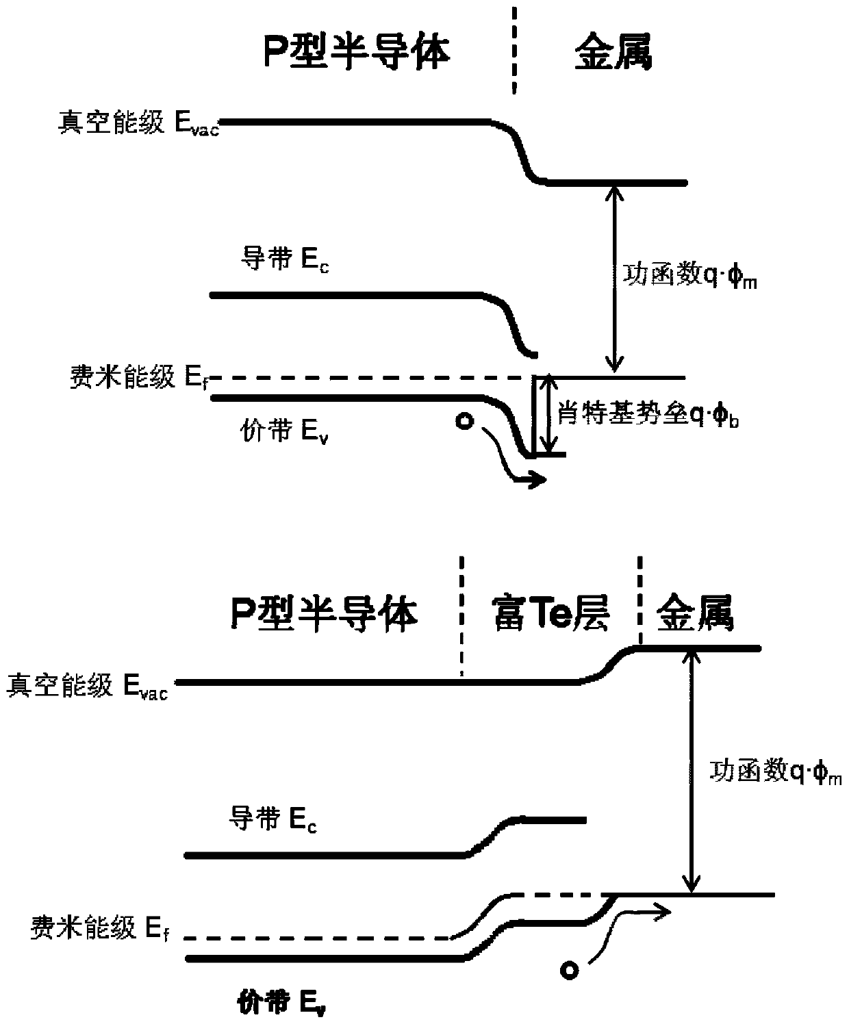
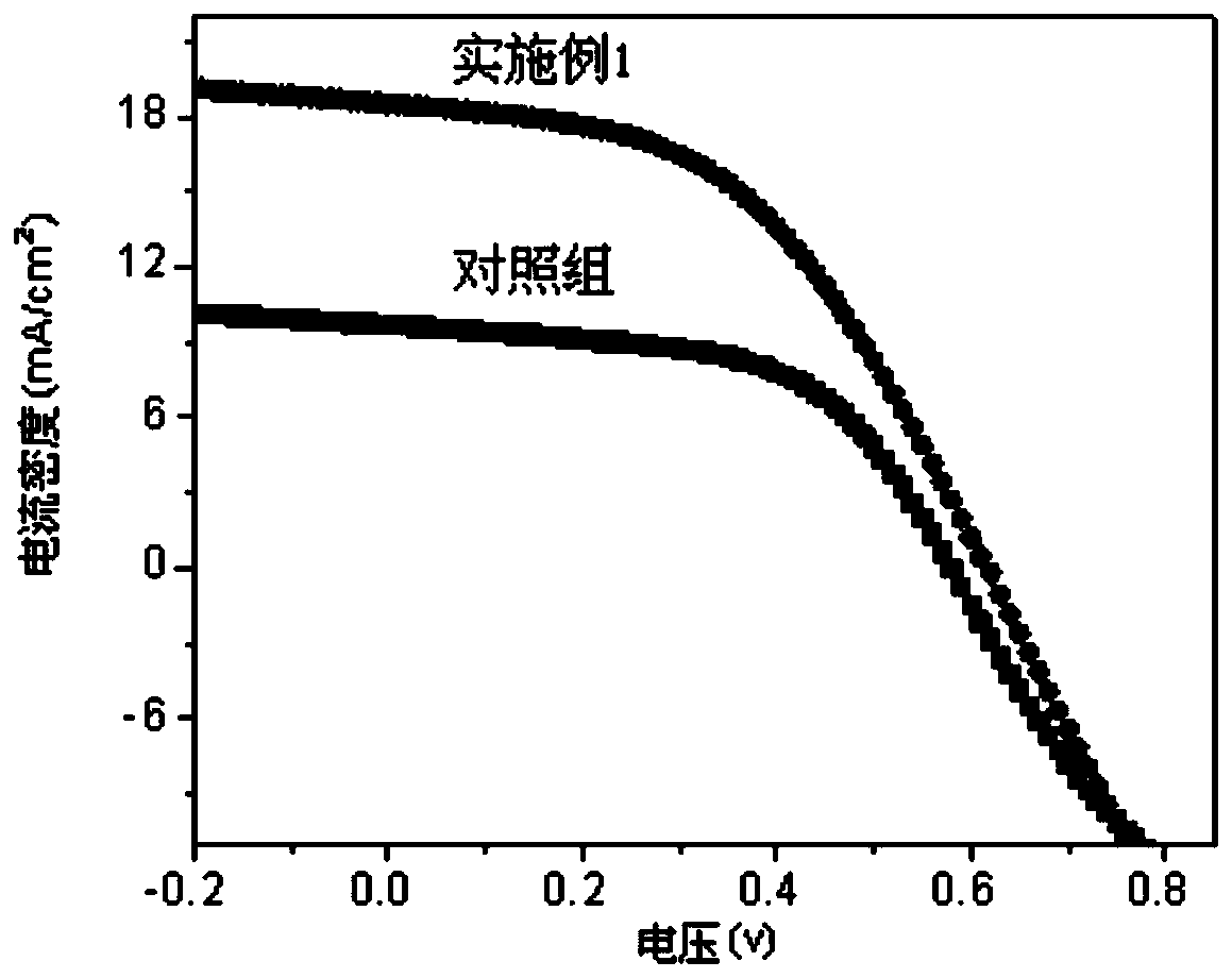
[0032] (1) CdTe nanocrystals (S.Sun, H.M.Liu, Y.P.Gao, D.H.Qin, J.Materials.Chemistry., 2012,517,6853-6856.) were prepared by solvothermal method, and then dissolved in an organic solvent to obtain Black solution, i.e. nanocrystalline solution, the nanocrystalline solution is deposited on the window layer (by sequentially stacked ITO glass substrate, ZnO layer, CdSe layer), then immersed in saturated methanol solution of cadmium chloride, treated at 350°C for a period of time to obtain a nanocrystalline monolayer, and then processed by layer-by-layer solution, which can effectively reduce interface defects and internal stress A uniform and dense photoactive layer (cadmium telluride nanocrystal thin film); the photoactive layer is formed by stacking one or more layers of cadmium telluride nanocrystals.
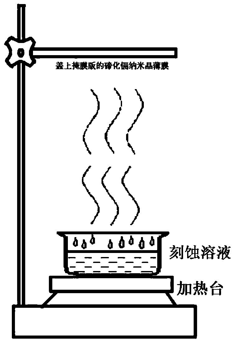
[0033] (2) Place the bromomethanol etching solution with a volume concentration of 5‰ on the heating stage, and place the cadmium telluride nanocrystalline film covered with th...
Embodiment 2
[0040] (1) CdTe nanocrystals (S.Sun, H.M.Liu, Y.P.Gao, D.H.Qin, J.Materials.Chemistry., 2012,517,6853-6856.) were prepared by solvothermal method, and then dissolved in an organic solvent to obtain Black solution, i.e. nanocrystalline solution, the nanocrystalline solution is deposited on the window layer (by sequentially stacked ITO glass substrate, ZnO layer, CdSe layer), then immersed in saturated methanol solution of cadmium chloride, treated at 350°C for a period of time to obtain a nanocrystalline monolayer, and then processed by layer-by-layer solution, which can effectively reduce interface defects and internal stress A uniform and dense photoactive layer (cadmium telluride nanocrystal thin film); the photoactive layer is formed by stacking one or more layers of cadmium telluride nanocrystals.
[0041] (2) Put the phosphoric acid nitric acid mixed etching solution (nitric acid: phosphoric acid: water = 1:70:29, volume ratio) on the heating stage, and place the cadmium ...
Embodiment 3
[0048] (1) CdTe nanocrystals (S.Sun, H.M.Liu, Y.P.Gao, D.H.Qin, J.Materials.Chemistry., 2012,517,6853-6856.) were prepared by solvothermal method, and then dissolved in an organic solvent to obtain Black solution, i.e. nanocrystalline solution, the nanocrystalline solution is deposited on the ITO glass substrate by spin coating, brush coating, spray coating, printing (preferably screen printing) or inkjet printing, and then immersed in saturated methanolic cadmium chloride solution Treatment, high temperature treatment at 350°C for a period of time to obtain a nanocrystalline monolayer, and then solution processing by layer-by-layer superposition to obtain a uniform and dense cadmium telluride nanocrystalline film that can effectively reduce interface defects and internal stress.
[0049] (2) Put the bromomethanol etching solution with a volume concentration of 1‰ on the heating stage, and place the cadmium telluride nanocrystalline film covered with the mask horizontally above...
PUM
| Property | Measurement | Unit |
|---|---|---|
| thickness | aaaaa | aaaaa |
| electron work function | aaaaa | aaaaa |
Abstract
Description
Claims
Application Information
 - R&D
- Intellectual Property
- Life Sciences
- Materials
- Tech Scout
- Unparalleled Data Quality
- Higher Quality Content
- 60% Fewer Hallucinations
Browse by: Latest US Patents, China's latest patents, Technical Efficacy Thesaurus, Application Domain, Technology Topic, Popular Technical Reports.
© 2025 PatSnap. All rights reserved.Legal|Privacy policy|Modern Slavery Act Transparency Statement|Sitemap|About US| Contact US: help@patsnap.com