A flash memory based on halogen perovskite material and a preparation method thereof

A perovskite material, a technology of flash memory, applied in the field of memory, can solve the problems of poor stability, slow read and write speed of flash memory, poor light regulation, etc., to achieve improved stability, excellent light response and light regulation characteristics, high The effect of charge carrier mobility

Inactive Publication Date: 2018-12-25
SHENZHEN UNIV
View PDF5 Cites 3 Cited by
  • Summary
  • Abstract
  • Description
  • Claims
  • Application Information

AI Technical Summary

Problems solved by technology

[0004] In view of the above-mentioned deficiencies in the prior art, the object of the present invention is to provide a flash memory based on a halogen perovskite material and a preparation method thereof, so as to solve the problems of slow reading and writing speed, poor light controllability and The problem of poor stability

Method used


Image

  • A flash memory based on halogen perovskite material and a preparation method thereof
  • A flash memory based on halogen perovskite material and a preparation method thereof
  • A flash memory based on halogen perovskite material and a preparation method thereof

Examples


preparation example Construction

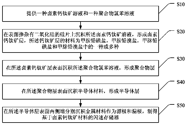
[0041] Based on the above-mentioned flash memory, the present invention also provides a preparation method of a flash memory based on a halogen perovskite material, wherein, as figure 2 shown, including steps:

[0042] S10, providing a kind of halogen perovskite solution and a kind of polymer chlorobenzene solution;

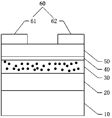
[0043] S20. Deposit the halogen perovskite solution on a silicon wafer doped with silicon dioxide on the surface to form a halogen perovskite layer. The material of the perovskite layer is methylamine lead iodide salt, methylamine lead bromide salt, formazan One or more of amidine lead iodide salt and formamidine lead bromide salt;

[0044] S30, depositing the polymer chlorobenzene solution on the surface of the halogen perovskite layer to form a polymer layer;

[0045] S40, depositing a semiconductor material on the surface of the polymer layer to form a semiconductor layer;

[0046] S50. Depositing metal materials on both sides of the surface of the semicon...

Embodiment 1

[0060] CH 3 NH 3 I(MAI) and PbI 2 MAPbI can be obtained by dissolving in dimethylformamide (DMF) at a ratio of 1:1. 3 Solution: Polymethyl methacrylate (PMMA) powder is dissolved in the chlorobenzene solution according to a certain ratio, and the mixed solution is placed in an ultrasonic machine so that PMMA is evenly dispersed in the solution to obtain a PMMA chlorobenzene solution.

[0061] The prepared MAPbI 3 The solution was spin-coated on the cleaned silicon wafer with 100nm silicon dioxide on the surface at 3000rpm for 40s, and annealed at 120°C for 40min after spin-coating to completely remove the residual solvent to obtain a halogen perovskite layer.

[0062] A uniform PMMA chlorobenzene solution was spin-coated on the surface of the halogen perovskite layer at 3000 rpm for 40 s, and annealed at 120° C. for 30 min after spin-coating to obtain a polymer layer.

[0063] Pentacene of about 30nm in 10 at a rate of 0.1 Å / s -6 In the form of thermal evaporation under T...

Embodiment 2

[0066] CH 3 NH 3 Br(MABr) and PbBr 2 MAPbBr can be obtained by dissolving in dimethylformamide (DMF) at a ratio of 1:1. 3 Solution: dissolving polystyrene (PS) powder in a certain proportion in a chlorobenzene solution, placing the mixed solution in an ultrasonic machine so that PS is evenly dispersed in the solution to obtain a PS chlorobenzene solution.

[0067] The prepared MAPbBr 3 The solution was spin-coated on the cleaned silicon wafer with 100nm silicon dioxide on the surface at 3200rpm for 45s, and annealed at 140°C for 45min after spin-coating to completely remove the residual solvent to obtain a halogen perovskite layer.

[0068] A uniform PS chlorobenzene solution was spin-coated on the surface of the halogen perovskite layer at a speed of 3500 rpm for 45 seconds, and annealed at a temperature of 150° C. for 35 minutes after the spin-coating to obtain a polymer layer.

[0069] Pentacene of about 30nm in 10 at a rate of 0.1 Å / s -6 In the form of thermal evapor...


PUM


Abstract

The invention discloses a flash memory based on halogen perovskite material and a preparation method thereof, wherein the flash memory comprises a rigid base electrode, a dielectric layer, a halogen perovskite layer, a polymer layer, a semiconductor layer and a metal thin film top electrode arranged in order from bottom to top, and the halogen perovskite layer is made of one or more of methylaminelead iodide salt, methylamine lead bromide salt, formamidine lead iodide salt and formamidine lead bromide salt. The halogen perovskite layer and the polymer layer are used as floating gate layers ofthe flash memory, so that the flash memory based on the halogen perovskite material has excellent light response and light control characteristics. At the same time, the polymer layer spin-coated onthe halogen perovskite layer can protect the halogen perovskite material and improve the stability of the device. Thus, the flash memory based on the halogen perovskite material of the present invention not only provides an efficient cumulative optical record programmable function and an electric erasing mode process, but also has a precise and stable light adjustable performance.

Description

technical field [0001] The invention relates to the field of memory, in particular to a flash memory based on a halogen perovskite material and a preparation method thereof. Background technique [0002] Flash memory is a memory based on field effect transistors, which mainly uses the floating gate layer in the transistor to capture and release carriers to store information. It has the characteristics of non-volatility, high reliability, low power consumption, high density, and low cost, and the stored content is electrically erasable and rewritable. Therefore, flash memory technology has developed rapidly. It has broad application prospects in portable storage such as U disk. The structure of the flash memory is based on the gate / dielectric layer / semiconductor layer / source-drain structure of a simple transistor, and an additional floating gate layer and an ultra-thin insulating layer are added to the dielectric layer / semiconductor layer, thereby Achieve non-volatility of ...

Claims


Application Information

Patent Timeline
Patent Type & Authority Applications(China)
IPC IPC(8): H01L51/30H01L51/05H01L51/40
CPCH10K71/00H10K10/471H10K10/474H10K10/466H10K2102/00
Inventor 韩素婷周晔王燕王展鹏陈锦锐
Owner SHENZHEN UNIV
Why Eureka
Try Eureka