

A kind of gradient nano-twinned copper bulk material and its temperature control preparation method
A nano-twinned copper and bulk material technology, applied in nanotechnology, instruments, electrolytic components, etc., can solve the problem that copper materials are difficult to combine strength and toughness, and achieve high strength, high conductivity, high strength and uniform plasticity. Effect
- Summary
- Abstract
- Description
- Claims
- Application Information
AI Technical Summary
Problems solved by technology
Method used
Image

Examples
Embodiment 1
[0040] 1. Fabrication of thin-sheet gradient nano-twinned copper materials by direct current electrolytic deposition
[0041] Electrolytic deposition equipment: DC stabilized voltage and stabilized current power supply;
[0042] Requirements for the electrolyte used in electrolytic deposition: CuSO with MOS grade purity 4 Solution, strictly control the metal impurity content of the electrolyte, the water used for distributing the electrolyte should be high-purity deionized water, use analytical pure H 2 SO 4 Adjust the pH value of the electrolyte solution, and the pH value of the electrolyte solution is 1.
[0043] In the above CuSO 4 Add the following additives to the solution:
[0044]A gelatin aqueous solution with a concentration of 5wt.% prepared by analytically pure gelatin, the addition amount is 1mL / L;
[0045] The concentration of 10wt.% NaCl aqueous solution prepared by using high-purity NaCl, the addition amount is 0.6mL / L.
Embodiment 2
[0052] The difference from Example 1 is:
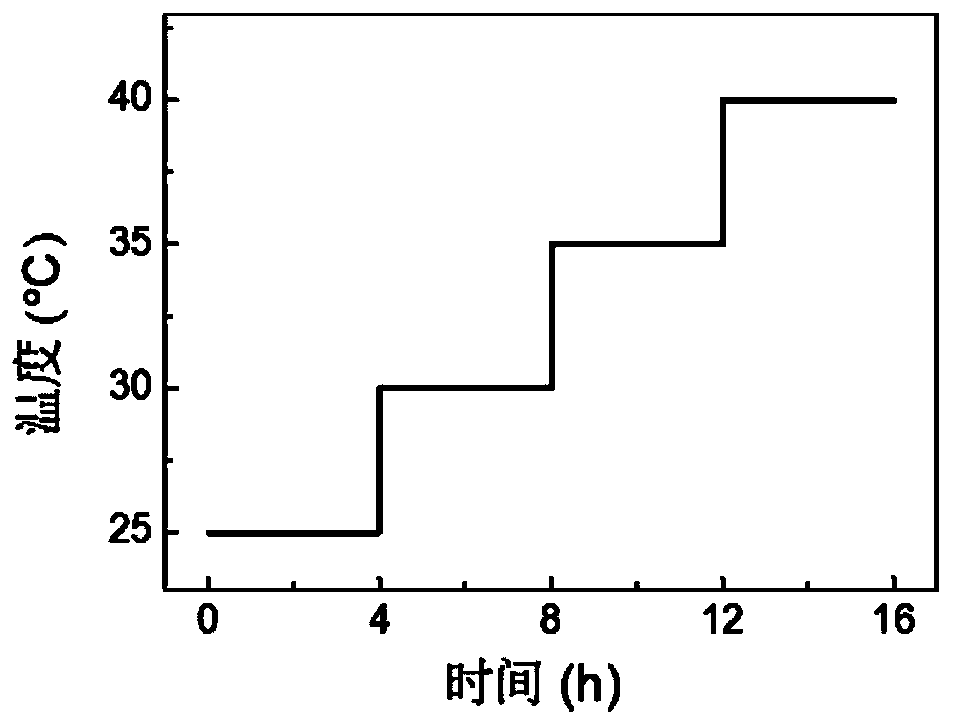
[0053] In the process of electrolytic deposition of gradient nano-twinned copper samples, the temperature of the electrolyte is controlled by heating with a magnetic stirrer, and the electrolyte is raised from 25°C to 40°C. During the heating process, the temperature is kept at 5°C for 2 hours; at 40°C for 4 hours After 1 hour, it is lowered to 25 °C, and it is kept at 5 °C for 2 hours during the cooling process, such as Figure 5 As shown, the electrolytic deposition time is 16h.
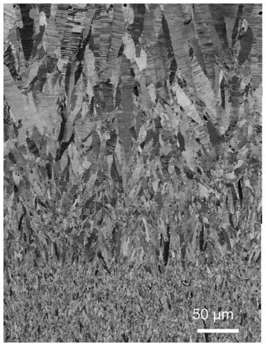
[0054] The prepared high-purity, high-density, flake-like gradient nano-twinned copper material has a thickness of 0.4 mm. Along the thickness direction (or with the temperature increasing first and then decreasing), the grain size and twinned layer thickness of the material all present A symmetric gradient change that first increases and then decreases, such as Figure 6 shown.
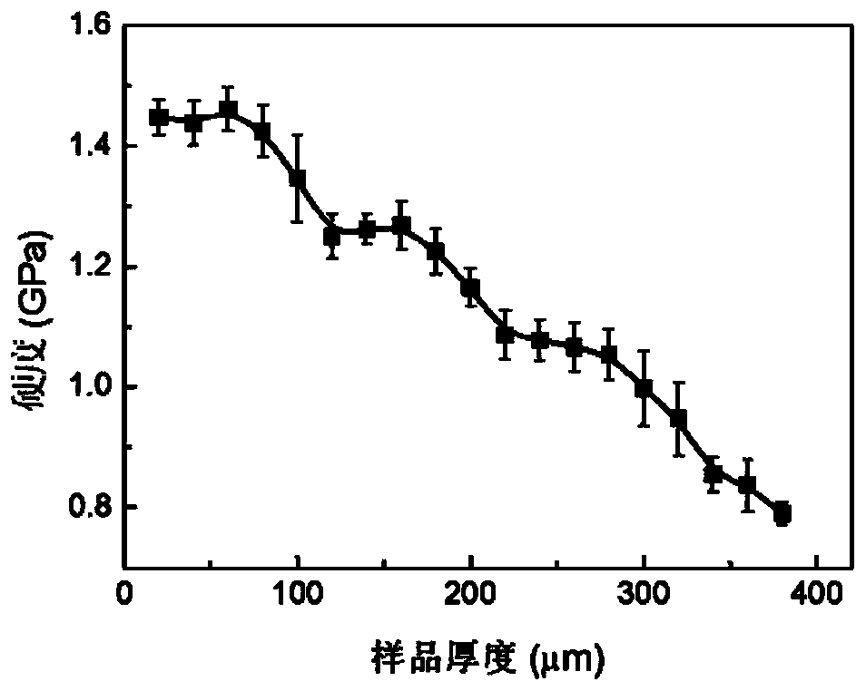
[0055] In this embodiment, the cross-sectional hardness of the gradient n...
Embodiment 3
[0058] The difference from Example 1 is:
[0059] In the process of electrolytic deposition of gradient nano-twinned copper samples, the temperature of the electrolyte is controlled by heating with a magnetic stirrer, and the electrolyte is raised from 25°C to 40°C. Reduce to 25°C after 1 hour, keep warm for 1 hour every 5°C during the cooling process, and then repeat this cooling method once, the temperature control curve is as follows Figure 8 As shown, the electrolytic deposition time is 16h.
[0060] The prepared high-purity, high-density, flake-like gradient nano-twinned copper material has a thickness of 0.4 mm. Along the thickness direction, the grain size and the thickness of the twinned wafer layer of the material show two-cycle symmetrical gradient changes. Its microstructure Figure such as Figure 9 shown.
[0061] In this embodiment, the cross-sectional hardness of the gradient nano-twinned copper material presents a two-period symmetrical gradient change with ...
PUM
| Property | Measurement | Unit |
|---|---|---|
| size | aaaaa | aaaaa |
| thickness | aaaaa | aaaaa |
| density | aaaaa | aaaaa |
Abstract
Description
Claims
Application Information