A full back electrode cell and its high-efficiency light trapping and selective doping manufacturing method
A technology of full back electrode and manufacturing method, which is applied in the direction of final product manufacturing, sustainable manufacturing/processing, circuits, etc., can solve the problems of high current density and imperfect long-wave band, and achieve low cost, good surface passivation effect, The effect of excellent light trapping structure
- Summary
- Abstract
- Description
- Claims
- Application Information
AI Technical Summary
Problems solved by technology
Method used
Image

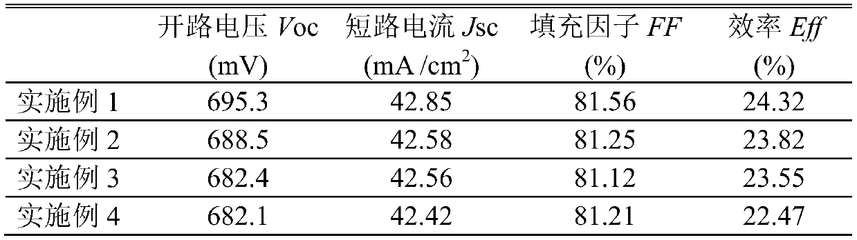
Examples
Embodiment 1
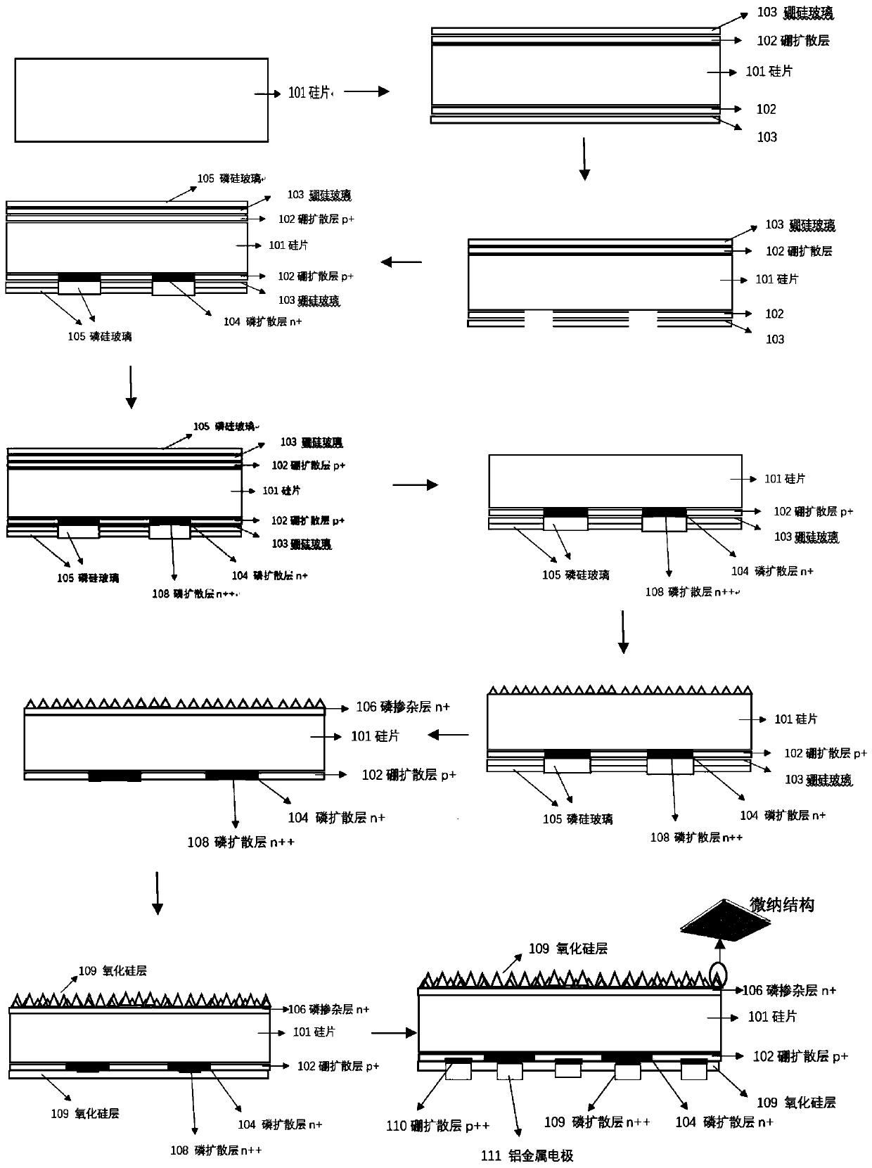
[0031] (1), select an n-type single crystal silicon wafer with a resistivity of 2.5Ωcm, use a high-concentration (20%) NaOH etching solution, polish it at a temperature of 90° C. for 1 minute, and clean it with a mixed solution of HF and HCl for 2 minutes;
[0032] (2), using BBr 3 The source is doped with boron, pre-deposition parameters: 800°C, 20min, N 2 The air flow is 13slm,O 2 Airflow 1500sccm, BBr 3 The flow rate is 150sccm, forming p on the entire silicon wafer surface + At the same time, a layer of borosilicate glass (BSG) dielectric layer is formed on the surface of the silicon wafer.
[0033] (3) Use a picosecond laser to remove the BSG and p-type layers on the surface of the area that needs to be doped with phosphorus on the back, and clean it with deionized water to remove some floating dust formed by laser irradiation;
[0034] (4), with POCl 3 Perform phosphorous doping, pre-deposit 700°C, 40min, N 2 The air flow is 15slm,O 2 Airflow 1800sccm, POCl 3 The...
Embodiment 2
[0046] Preparation:
[0047] Step (2), utilize BBr 3 Source for boron doping, pre-deposition parameters: 750°C, 25min, N 2 The air flow is 13slm,O 2 Airflow 1500sccm, BBr 3 The flow rate is 150sccm, the high temperature propulsion temperature is 1000°C, and the propulsion time is 15min;
[0048] Step (4), with POCl 3 Phosphorus doping, pre-deposition 800°C, 40min, N 2 The air flow is 15slm,O 2 Airflow 1800sccm, POCl 3 The flow rate is 400 sccm. The advancing temperature is 950°C, and the advancing time is 10 minutes.
[0049] Others are the same as embodiment 1.
Embodiment 3
[0051] Preparation:
[0052] Step (11), using the atomic layer deposition (ALD) method to simultaneously prepare an ultra-thin silicon oxide layer on the front and back, specifically: first pass trimethylsilane into the deposition chamber for 10 seconds, and then inject Access to N 2 Gas, purge time 10s. Ozone O was introduced into the chamber 3 , the passage time is 10s, and then pass N into the chamber 2 gas, the purge time is 10s, and the deposition temperature is 300°C. This is a cycle. Repeat 300 times.
[0053] Others are the same as embodiment 1
PUM
 Abstract
Description
Claims
Application Information