Application of zinc titanate in crystalline silicon solar cell

A technology of crystalline silicon solar cells and zinc titanate, which is applied in the direction of circuits, photovoltaic power generation, electrical components, etc., can solve the problems of reducing device photogenerated current, narrow density band gap, and restricting spectral response, so as to increase photogenerated current and reduce Effect of parasitic absorption, good carrier transport

Pending Publication Date: 2022-04-05
JIANGSU OCEAN UNIV
View PDF0 Cites 0 Cited by
  • Summary
  • Abstract
  • Description
  • Claims
  • Application Information

AI Technical Summary

Problems solved by technology

[0004] The above battery structures need to rely on heavily doped amorphous silicon, polycrystalline silicon or microcrystalline silicon to achieve electronic selective contact. Although these battery structures show high photoelectric conversion efficiency, whether it is amorphous silicon thin film, polycrystalline Silicon thin films, which have a high density of defect states and a narrow band gap, are likely to cause significant parasitic light absorption, which restricts the improvement of the spectral response, reduces the photogenerated current of the device, and affects the further improvement of the conversion efficiency.
In addition, this doping process also requires high temperature and highly toxic gases (borane, phosphine and silane) to grow, the process is complicated and the cost is high

Method used


Image

  • Application of zinc titanate in crystalline silicon solar cell
  • Application of zinc titanate in crystalline silicon solar cell
  • Application of zinc titanate in crystalline silicon solar cell

Examples


Embodiment 1

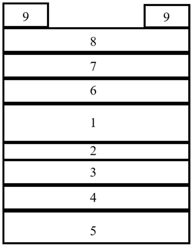
[0034] The schematic diagram of the structure of the crystalline silicon solar cell prepared in this example is shown in figure 2 ,in:

[0035] 1 is a crystalline silicon substrate, specifically an N-type crystalline silicon substrate (P-type has the same technical effect), with a thickness of 300 μm;

[0036] 2 is the lower passivation film, covering the entire lower surface of the crystalline silicon substrate, with a thickness of 10nm;

[0037] 3 is a zinc titanate electron selective layer covering the entire lower passivation film with a thickness of 100nm;

[0038] 4 is the lower transparent conductive film, covering the entire zinc titanate electron selective layer, with a thickness of 80nm;

[0039] 5 is the lower metal electrode layer, covering the entire lower transparent conductive film, with a thickness of 500nm;

[0040] 6 is an upper passivation film layer, covering the entire upper surface of the crystalline silicon substrate, with a thickness of 10nm;

[00...

Embodiment 2

[0053] (1) Pretreat the P-type crystalline silicon substrate by wet chemical method, including polishing, cleaning, and texturing; the specific steps are as follows: first, the silicon wafer is put into a NaOH solution with a concentration of 10%. Wash at ℃ for 15 minutes to remove the damaged layer of the silicon wafer, that is, to polish; secondly, put the silicon wafer with the damaged layer in 3% KOH alkali solution for 10 minutes, and use the alkali solution to etch different crystal faces The difference in speed is used for random pyramid texturing on the surface to form randomly distributed pyramid textures; finally, the RCA cleaning process is used to put the silicon wafer into a mixed aqueous solution of hydrochloric acid and hydrogen peroxide, and the solution ratio is HCl:H 2 o 2 :H 2 O=1:1:5, temperature 80°C, soak for 10min to remove metal ions.

[0054] (2) Use plasma enhanced chemical vapor deposition (PECVD) to SiH 4 、H 2 As a reaction gas, an intrinsic hyd...

Embodiment 3

[0061] (1) N-type crystalline silicon substrate is pretreated by wet chemical method, including polishing, cleaning, and texturing; the specific steps are as follows: first, the silicon wafer is put into a NaOH solution with a concentration of 10%. Wash at ℃ for 15 minutes to remove the damaged layer of the silicon wafer, that is, to polish; secondly, put the silicon wafer with the damaged layer in 3% KOH alkali solution for 10 minutes, and use the alkali solution to etch different crystal faces The difference in speed is used for random pyramid texturing on the surface to form randomly distributed pyramid textures; finally, the RCA cleaning process is used to put the silicon wafer into a mixed aqueous solution of hydrochloric acid and hydrogen peroxide, and the solution ratio is HCl:H 2 o 2 :H 2 O=1:1:5, temperature 80°C, soak for 10min to remove metal ions.

[0062] (2) Use plasma enhanced chemical vapor deposition (PECVD) to SiH 4 、H 2 As a reaction gas, an intrinsic hy...


PUM

PropertyMeasurementUnit
thicknessaaaaaaaaaa
thicknessaaaaaaaaaa
thicknessaaaaaaaaaa

Abstract

The invention relates to a crystalline silicon solar cell, in particular to application of zinc titanate in the crystalline silicon solar cell. The zinc titanate film is used as an electron selection layer in the crystalline silicon solar cell, the zinc titanate film has an energy band structure matched with a crystalline silicon substrate, a small conduction band order and a large valence band order can be generated when the zinc titanate film makes contact with crystalline silicon, electrons can be effectively selected on a contact interface, holes can be effectively blocked, and therefore zinc titanate/crystalline silicon heterogeneous contact is achieved, and the solar cell efficiency is improved. And the excellent electron selectivity is shown. The zinc titanate thin film also has a lower work function, and when the zinc titanate thin film is in contact with a crystalline silicon substrate, a crystalline silicon energy band is induced to be bent, so that electrons can be transmitted from crystalline silicon to zinc titanate.

Description

technical field [0001] The invention relates to crystalline silicon solar cells, in particular to the application of zinc titanate in crystalline silicon solar cells. Background technique [0002] Carrier selective contact is a research hotspot in high-efficiency crystalline silicon solar cells, aiming at the efficient separation and collection of photogenerated electron-hole pairs. Therefore, the performance of carrier selective contact directly affects the performance of solar cells. The carrier-selective contact includes electron-selective contact and hole-selective contact, where electron-selective contact facilitates electron transport but hinders hole transport, and hole-selective contact does the opposite. [0003] At present, in the industry, heavy doping is mainly used to realize electronic selective contact of crystalline silicon solar cells. Including (1) passivated emitter and rear (PERC) cells: high-temperature phosphorus diffusion is performed in the crystall...

Claims


Application Information

Patent Timeline
Patent Type & Authority Applications(China)
IPC IPC(8): H01L31/032H01L31/074H01L31/18C01G9/00C01G23/00
CPCY02E10/50Y02P70/50
Inventor 钟思华王广一张文春焦泽栋贾保平毛日骏岳宗毅
Owner JIANGSU OCEAN UNIV
Why Eureka
Try Eureka