An ordered heterojunction photovoltaic device and a preparation method thereof

A photovoltaic device and heterojunction technology, which is applied in the direction of organic semiconductor devices, semiconductor/solid-state device manufacturing, photovoltaic power generation, etc., can solve the problems that affect the conversion efficiency of photovoltaic devices, complex preparation process, poor regularity, etc., to reduce charge recombination probability, simplification of photovoltaic device structure, and reduction of manufacturing cost

Pending Publication Date: 2019-01-18
UNIV OF ELECTRONICS SCI & TECH OF CHINA ZHONGSHAN INST
View PDF0 Cites 5 Cited by
  • Summary
  • Abstract
  • Description
  • Claims
  • Application Information

AI Technical Summary

Problems solved by technology

[0003] The patent document with the publication number "104617221A" discloses an organic-inorganic hybrid solar cell and its preparation method. The technical scheme adopted is: growing TiO on FTO conductive glass 2 Nanorod arrays, TiO 2 The surface of the nanorod array is adsorbed with triphenylamine dye and spin-coated with P3HT, PEDOT:PSS film coated TiO 2 The surface of the nanorod array constitutes a hole transport layer, and metal Au is vapor-deposited on the PEDOT:PSS film. This solar cell has a high photoelectric conversion efficiency, but it needs to absorb photosensitizers on the surface of the nanorod array, and the preparation process is complicated. cost
[0004] The patent document with the publication number "103219468B" discloses an ordered bulk heterojunction organic solar cell and its preparation method. The technical scheme adopted is: obtain a molecular template layer by vacuum deposition or solution spin coating deposition, and obtain a molecular template layer by oblique Angle-incidence vacuum deposition prepares the nanorod array thin film layer, then spin-coats the active layer material, and vacuum-deposits the electrode buffer layer and metal electrode, which effectively simplifies the preparation steps of the solar cell. However, the nanorod array is prepared at an oblique angle, and its regularity The degree is poor, which will affect the conversion efficiency of photovoltaic devices

Method used


Image

  • An ordered heterojunction photovoltaic device and a preparation method thereof
  • An ordered heterojunction photovoltaic device and a preparation method thereof
  • An ordered heterojunction photovoltaic device and a preparation method thereof

Examples


Embodiment 1

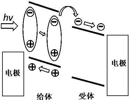
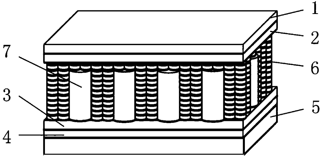
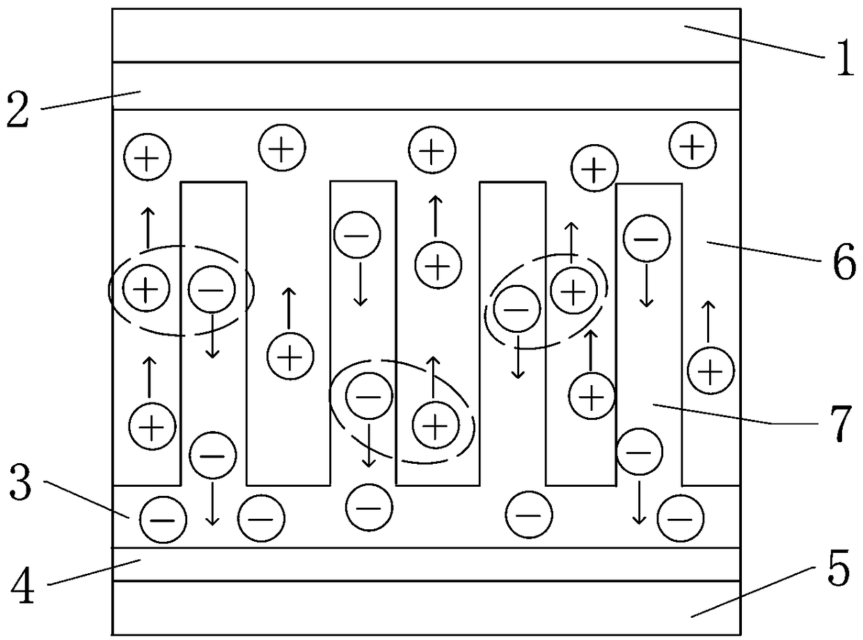
[0038] An ordered heterojunction photovoltaic device, from top to bottom is a cathode layer 1, an interface modification layer 2, a photovoltaic active layer, a hole blocking layer 3, an anode layer 4 and a substrate 5. The negative electrode layer 1 is an Au film with a thickness of 100 nm; the interface modification layer 2 is a MoO film with a thickness of 10 nm. 3 Thin film; The photovoltaic active layer includes an organic layer 6 and an inorganic layer; The hole blocking layer 3 is a ZnO thin film with a thickness of 10nm; The positive electrode layer 4 is an FTO electrode; The substrate 5 is a glass substrate.

[0039]The inorganic layer is an ordered ZnO nanorod array perpendicular to the substrate 5, the organic layer 6 fills and covers the ZnO nanorod array, and the top surface of the organic layer 6 is in contact with the substrate. 5 in parallel, the organic layer 6 is made of perylene liquid crystal PE-TP, the nanorods in the ZnO nanorod array have a height of 400...

Embodiment 2

[0050] An ordered heterojunction photovoltaic device comprises a cathode layer 1, an interface modification layer 2, a photovoltaic active layer, a hole blocking layer 3, an anode layer 4 and a substrate 5 from top to bottom. The negative electrode layer 1 is an Au film with a thickness of 150 nm; the interface modification layer 2 is a MoO film with a thickness of 50 nm. 3 Thin film; The photovoltaic active layer includes an organic layer 6 and an inorganic layer; The hole blocking layer 3 is a ZnO thin film with a thickness of 30nm; The positive electrode layer 4 is an FTO electrode; The substrate 5 is a glass substrate.

[0051] The inorganic layer is an ordered ZnO nanorod array perpendicular to the substrate 5, the organic layer 6 fills and covers the ZnO nanorod array, and the top surface of the organic layer 6 is in contact with the substrate. 5 parallel, the organic layer 6 is made of perylene liquid crystal PE-TP, the nanorods in the ZnO nanorod array have a height of...

Embodiment 3

[0054] An ordered heterojunction photovoltaic device, from top to bottom is a cathode layer 1, an interface modification layer 2, a photovoltaic active layer, a hole blocking layer 3, an anode layer 4 and a substrate 5. The negative electrode layer 1 is an Au film with a thickness of 150 nm; the interface modification layer 2 is a MoO film with a thickness of 50 nm. 3 Thin film; The photovoltaic active layer includes an organic layer 6 and an inorganic layer; The hole blocking layer 3 is a ZnO thin film with a thickness of 30nm; The positive electrode layer 4 is an FTO electrode; The substrate 5 is a glass substrate.

[0055] The inorganic layer is an ordered ZnO nanorod array perpendicular to the substrate 5, the organic layer 6 fills and covers the ZnO nanorod array, and the top surface of the organic layer 6 is in contact with the substrate. 5 in parallel, the organic layer 6 is made of perylene liquid crystal PE-TP, the nanorods in the ZnO nanorod array have a height of 30...


PUM


Abstract

The invention discloses an ordered heterojunction photovoltaic device and a preparation method thereof. the ordered heterojunction photovoltaic devices includes a negative layer, an interface modification layer, a photovoltaic active layer, a hole barrier layer, a positive electrode layer and a substrate from top to bottom, wherein the photovoltaic active layer comprises an organic layer and an inorganic layer, wherein the inorganic layer is an ordered nanorod array perpendicular to the substrate, the organic layer fills and covers the nanorod array, the top surface of the organic layer is parallel to the substrate, and the nanorod height in the nanorod array is 300-500 nm, and the diameter is 50-100 nm, and the distance between the nanorods is 60-80nm, the nanorod array and the organic layer of the invention intersect each other to form an ordered network structure, The photogenerated exciton dissociation surface can be ensured to be large, and the electrons and holes generated by thedissociation can be transported in the two transmission channels respectively, so that the hopping transmission of the carriers between the donor material particles and the acceptor material particles is avoided, the charge recombination probability is effectively reduced, and higher photoelectric conversion efficiency can be obtained.

Description

technical field [0001] The invention relates to a photovoltaic device, in particular to an ordered heterojunction photovoltaic device and a preparation method thereof. Background technique [0002] As a new type of renewable energy, solar energy is considered to be the most promising new energy and has received more and more attention and research. Photovoltaic technology directly converts sunlight into electrical energy without generating noise, toxic waste or greenhouse gases and is therefore seen as an attractive new energy technology. The organic-inorganic composite photovoltaic device is considered to be an ideal photovoltaic device structure because it combines the advantages of both organic materials and inorganic materials. Its working principle is as follows: figure 1 Shown: Under the irradiation of sunlight, the organic polymer material in the active layer of the photovoltaic device is excited by the incident light, absorbing photons and converting them into excit...

Claims


Application Information

Patent Timeline
Patent Type & Authority Applications(China)
IPC IPC(8): H01L51/42H01L51/46H01L51/48
CPCH10K71/12H10K71/40H10K85/731H10K30/152H10K2102/00Y02E10/549
Inventor 张智易子川杨健君刘黎明迟锋水玲玲
Owner UNIV OF ELECTRONICS SCI & TECH OF CHINA ZHONGSHAN INST
Why Eureka
Try Eureka