Silicon-based solar cell, preparation method and photovoltaic module

A solar cell, silicon-based technology, applied in the field of solar cells, can solve the problems of reducing cell photoelectric conversion efficiency, photoelectric conversion performance dependence, solar cell voltage and current loss, etc.

Pending Publication Date: 2019-03-19
JA SOLAR TECH YANGZHOU
View PDF0 Cites 17 Cited by
  • Summary
  • Abstract
  • Description
  • Claims
  • Application Information

AI Technical Summary

Problems solved by technology

The photoelectric conversion performance of silicon-based solar cells depends on its internal minority carrier concentration. The recombination annihilation of minority carriers will cause the loss of solar cell voltage and current, thereby reducing the photoelectric conversion efficiency of the cell.
[0003] There are many defects on the surface of the silicon wafer, which are very serious recombination centers

Method used


Image

  • Silicon-based solar cell, preparation method and photovoltaic module
  • Silicon-based solar cell, preparation method and photovoltaic module
  • Silicon-based solar cell, preparation method and photovoltaic module

Examples


Embodiment approach 1

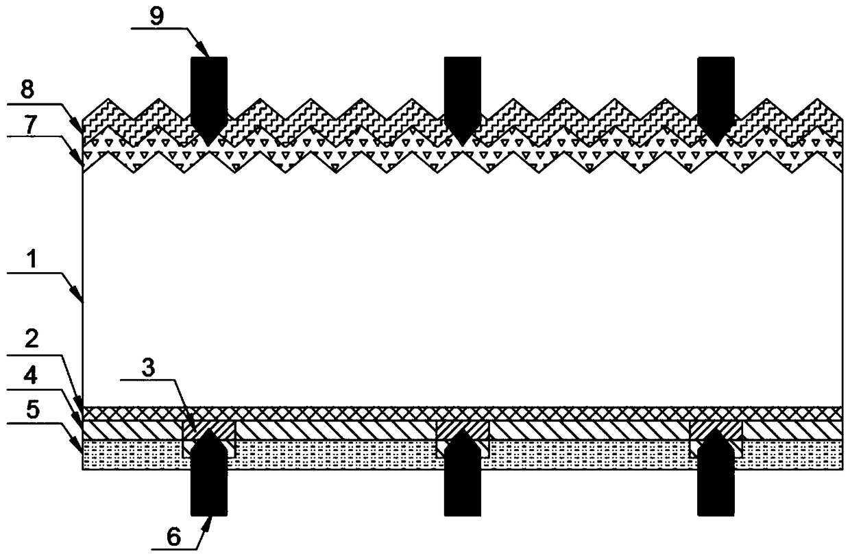
[0141] like figure 1 As shown, in this embodiment, the front side of the silicon-based solar cell includes:

[0142] The emitter layer 7 arranged on the front surface of the P-type crystalline silicon substrate 1,

[0143] an anti-reflection layer 8 disposed on the emitter layer 7,

[0144] as well as,

[0145] A front electrode 9 disposed on the anti-reflection layer 8 .

[0146] Wherein, the front electrode 9 is in ohmic contact with the emitter layer 7 through the anti-reflection layer 8 .

[0147] It can be understood that the emitter layer 7 is N-type silicon, which can be formed by doping the P-type crystalline silicon substrate 1 with group V elements (including but not limited to phosphorus). In this embodiment, the sheet resistance value of the emitter layer 7 formed after doping can be 40Ω / □~200Ω / □ (such as 40Ω / □, 50Ω / □, 60Ω / □, 70Ω / □, 80Ω / □, 90Ω / □ / □, 100Ω / □, 110Ω / □, 120Ω / □, 130Ω / □, 140Ω / □, 150Ω / □, 160Ω / □, 170Ω / □, 180Ω / □, 190Ω / □, 200Ω / □, etc.), emission The she...

Embodiment approach 2

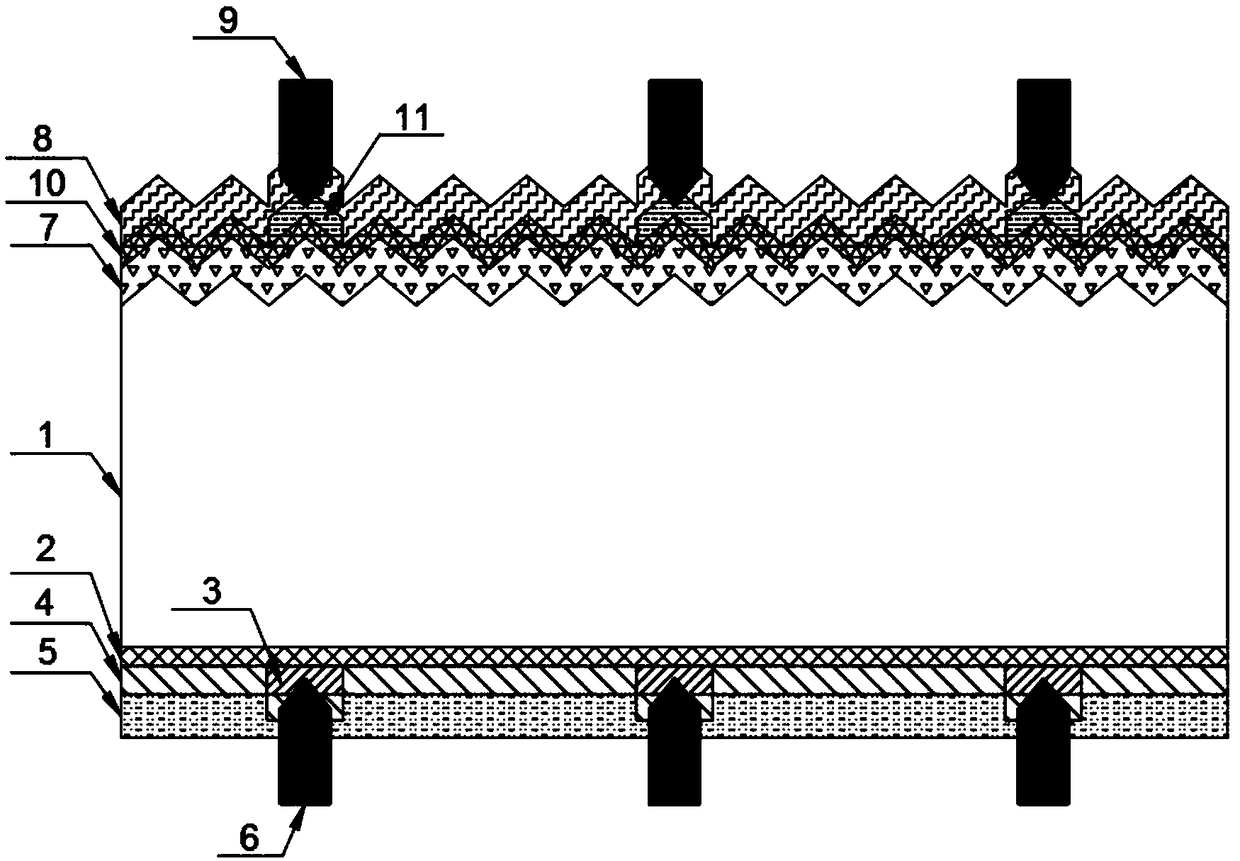
[0151] like figure 2 As shown, in this embodiment, the front side of the silicon-based solar cell includes:

[0152] The emitter layer 7 arranged on the front surface of the P-type crystalline silicon substrate 1,

[0153] a front tunneling passivation layer 10 arranged on the emitter layer 7,

[0154] a group V element-doped front-side doped silicon layer 11 disposed on a partial region of the front-side tunneling passivation layer 10,

[0155] anti-reflection layer 8 disposed on the front-side doped silicon layer 11 and on the region of the front-side tunneling passivation layer 10 where the front-side doped silicon layer 11 is not provided, and,

[0156] A front electrode 9 disposed on the anti-reflection layer 8 .

[0157] Wherein, the front electrode 9 is in ohmic contact with the front doped silicon layer 11 through the antireflection layer 8 .

[0158] In this embodiment, the structures of the emitter layer 7 , the anti-reflection layer 8 and the front electrode 9 ...

Embodiment 1

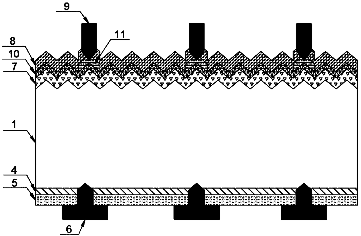
[0234] This embodiment provides a silicon-based solar cell passivated by gallium oxide, such as figure 1 As shown, the solar cell includes a P-type crystalline silicon substrate 1, an emitter layer 7 arranged on the front of the P-type crystalline silicon substrate 1, an antireflection layer 8 arranged on the emitter layer 7, and an antireflection layer 8 arranged on the antireflection layer 8. The front electrode 9 is arranged on the back tunnel passivation layer 2 on the back of the P-type crystalline silicon substrate 1, and the back doped polysilicon layer doped with boron element is arranged on the back tunnel passivation layer 2 corresponding to the region of the back electrode 6, The gallium oxide layer 4 arranged on the back doped polysilicon layer and the region of the back tunnel passivation layer 2 not provided with the back doped polysilicon layer, the covering layer 5 arranged on the gallium oxide layer 4, and the covering layer 5 arranged on the covering layer 5 ...


PUM


Abstract

The invention discloses a silicon-based solar cell, a preparation method and a photovoltaic module, which belong to the technical field of solar cells. The silicon-based solar cell comprises a P-typecrystalline silicon substrate, a back tunneling passivation layer arranged on the back of the P-type crystalline silicon substrate, a group III element doped back doped silicon layer arranged on a partial region of the back tunneling passivation layer, a gallium oxide layer, a coating layer arranged on the gallium oxide layer, and a back electrode arranged on the coating layer. The gallium oxide layer is arranged on the back doped silicon layer and a region without the back doped silicon layer on the back tunneling passivation layer. In the solar cell, the P-type silicon surface is chemicallypassivated and field-passivated by negative charges carried by the gallium oxide layer. The number of dangling bonds and minority carriers of silicon atoms on the P-type silicon surface is reduced. The recombination rate of minority carriers is reduced. The voltage and current of the solar cell are improved. The photoelectric conversion efficiency of the solar cell is improved.

Description

technical field [0001] The invention relates to the technical field of solar cells, in particular to a silicon-based solar cell, a preparation method, and a photovoltaic module. Background technique [0002] Photovoltaic power generation, which directly converts solar energy into electricity, is a clean, sustainable and relatively cost-effective way of generating electricity. Silicon-based solar cells are an important part of photovoltaic power generation systems. The photoelectric conversion efficiency of silicon-based solar cells has an important impact on the output power and cost of electricity of photovoltaic power generation. The photoelectric conversion performance of silicon-based solar cells depends on its internal minority carrier concentration, and the recombination annihilation of minority carriers will cause the loss of solar cell voltage and current, thereby reducing the photoelectric conversion efficiency of the cell. [0003] There are many defects on the su...

Claims


Application Information

Patent Timeline
Patent Type & Authority Applications(China)
IPC IPC(8): H01L31/0216H01L31/0224H01L31/028H01L31/042H01L31/18
CPCH01L31/02167H01L31/02168H01L31/022425H01L31/028H01L31/042H01L31/1804Y02E10/547Y02P70/50
Inventor 陈孝业薛文娟
Owner JA SOLAR TECH YANGZHOU
Why Eureka
Try Eureka