N-type organic semiconductor material as well as preparation method and application thereof
An organic semiconductor, n-type technology, applied in the field of n-type organic semiconductor materials and their preparation, can solve problems such as poor light absorption ability, difficulty in regulating physical and chemical properties due to fixed structure, and limited practical application prospects of fullerene acceptor materials.
- Summary
- Abstract
- Description
- Claims
- Application Information
AI Technical Summary
Problems solved by technology
Method used
Image

Examples
Embodiment 1
[0165] This embodiment prepares the brominated monomer (compound 4) of the n-type organic semiconductor material having the structure shown in formula II through the following steps:
[0166] Step (1): Synthesis of Compound 2
[0167]
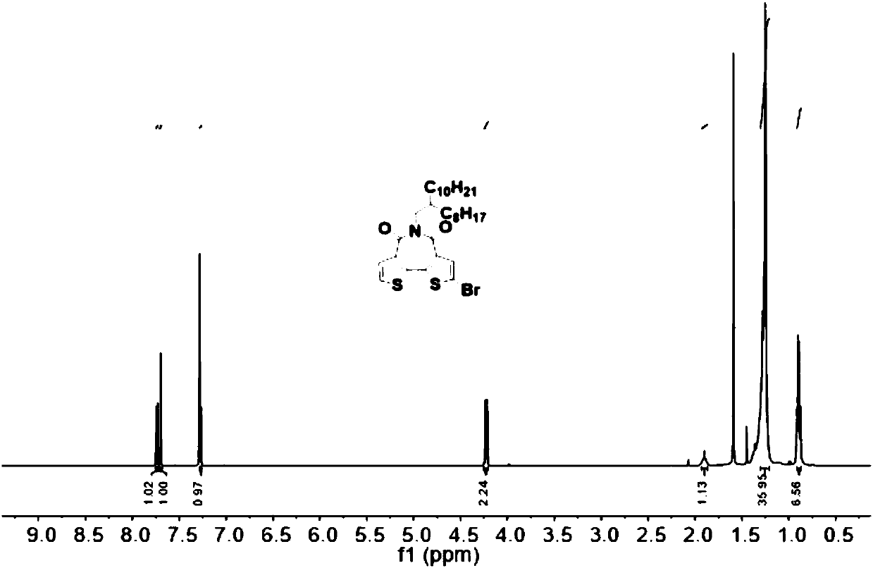
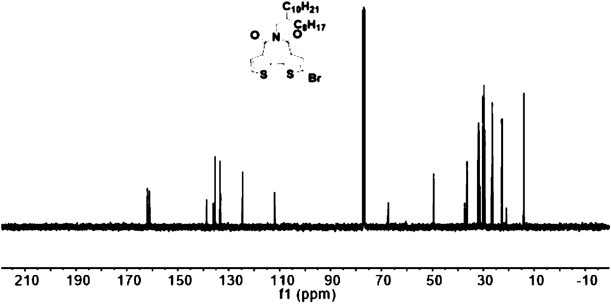
[0168] Compound 1 (1.03 g, 2.0 mmol) was dissolved in 20 mL of chloroform. Then add 320 mg of liquid bromine and 10 mg of ferric chloride. The reaction was carried out in the dark at room temperature overnight. After the reaction is complete, add sodium sulfite aqueous solution, stir vigorously for 30 minutes, extract, dry, and spin out the solvent to obtain the initial product, which is further purified by silica gel chromatography to obtain a white solid product 2 with a mass of 450 mg (yield 38%), nuclear magnetic resonance Hydrogen spectrum such as Figure 1A As shown, the carbon NMR spectrum is as Figure 1B shown.
[0169] 1 H NMR (400MHz, CDCl 3 )δ:7.74-7.73(d,1H),7.70(s,1H),7.28-7.27(d,1H),4.23-4.22(d,2H),1.90(s,1H),1.36-1.25(m...
Embodiment 2
[0179] This embodiment prepares the brominated monomer (compound 6) of the n-type organic semiconductor material having the structure shown in formula III through the following steps:
[0180] Synthesis of compound 6
[0181]
[0182] Compound 5 (130 mg, 0.129 mmol) was dissolved in 20 mL of chloroform. Add 44 mg of liquid bromine and 2 mg of ferric chloride. The reaction mixture was reacted for 12 hours in the dark. After the reaction was complete, an aqueous solution of sodium sulfite was added and stirred for 30 minutes. Extraction, drying and further purification by silica gel chromatography column to obtain yellow solid product 6, the quality is 130mg, the yield is 87%, and the hydrogen nuclear magnetic resonance spectrum is as follows: Figure 4A As shown, the carbon NMR spectrum is as Figure 4B shown.
[0183] 1 H NMR (400MHz, CDCl 3 )δ:7.80(s,2H),4.32-4.30(d,4H),1.96(s,2H),1.40-1.25(m,64H),0.90-0.86(m,12H). 13 C NMR (100MHz, CDCl 3 )δ:160.69,160.05,139.94,...
Embodiment 3
[0185] This embodiment prepares the brominated monomer (compound 8) of the n-type organic semiconductor material having the structure shown in formula IV through the following steps:
[0186]
[0187] Compound 7 (149 mg, 0.1 mmol) was dissolved in 20 mL of chloroform. Add 35 mg of liquid bromine and 2 mg of ferric chloride. The reaction mixture was reacted for 12 hours in the dark. After the reaction was complete, an aqueous solution of sodium sulfite was added and stirred for 30 minutes. Extraction, drying and further purification by silica gel chromatography until the yellow solid product 8, 153 mg, yield 92%, H NMR spectrum as Figure 5 shown.
[0188] 1 H NMR (400MHz, CDCl 3 )δ:7.53(s,2H),4.37-4.35(d,2H),4.31-4.29(d,4H),2.12(s,1),2.0(s,2H),1.40-1.27(m,96H) ,0.89-0.86(m,18H).
PUM
| Property | Measurement | Unit |
|---|---|---|
| Molecular weight | aaaaa | aaaaa |
Abstract
Description
Claims
Application Information
 - R&D
- Intellectual Property
- Life Sciences
- Materials
- Tech Scout
- Unparalleled Data Quality
- Higher Quality Content
- 60% Fewer Hallucinations
Browse by: Latest US Patents, China's latest patents, Technical Efficacy Thesaurus, Application Domain, Technology Topic, Popular Technical Reports.
© 2025 PatSnap. All rights reserved.Legal|Privacy policy|Modern Slavery Act Transparency Statement|Sitemap|About US| Contact US: help@patsnap.com