Electronic skin and preparation method and application thereof

An electronic skin and electrode technology, applied in the field of electronic skin and its preparation, can solve the problems of inability to meet the environmental requirements of electronic skin products, inability to withstand high temperature, low temperature natural environment, time-consuming and inability to semiconductor processes, etc., and achieve easy industrialization The effect of promotion, light weight and low power consumption

Active Publication Date: 2019-04-05
INT ACAD OF OPTOELECTRONICS AT ZHAOQING SOUTH CHINA NORMAL UNIV
View PDF9 Cites 3 Cited by
  • Summary
  • Abstract
  • Description
  • Claims
  • Application Information

AI Technical Summary

Problems solved by technology

However, some unavoidable problems limit the application of these traditional electronic skins. For example, stress sensors using carbon nanotubes and graphene as sensing materials require a transfer process during the preparation process, and electronic skins using metal nanowires as sensing materials are in The fabrication process requires electrospinning processes, which are time-consuming

Method used


Image

  • Electronic skin and preparation method and application thereof
  • Electronic skin and preparation method and application thereof
  • Electronic skin and preparation method and application thereof

Examples


Embodiment 1

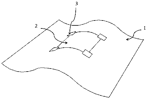
[0050] An electronic skin, such as figure 1 As shown, including mica substrate 1, 50% Nb-doped BaTiO covered on the mica substrate 3 The semiconductor film layer 2, the platinum electrode 3 covered on the semiconductor film layer, the thickness of the mica substrate is 0.5 μm, the thickness of the semiconductor film layer is 10nm, the thickness of the platinum electrode is 30nm, and the surface of the semiconductor film layer is atomically flat surface.

[0051] The preparation method of electronic skin comprises the following steps:

[0052] S1.50% Nb doped BaTiO 3 Preparation of thin film: with Ba 0.5 Nb 0.5 TiO 3 As a target, bombard Ba 0.5 Nb 0.5 TiO 3 The target makes the surface of the formed plasma-deposited mica substrate form Ba 0.5 Nb 0.5 TiO 3 Thin film, deposition conditions: 650°C, oxygen pressure 3.0×10 -4 Pa, laser energy flux density 1.5J cm -2 , the pulse frequency is 1Hz, and the distance between the target and the mica substrate is 45mm;

[005...

Embodiment 2

[0064] An electronic skin, such as figure 1 As shown, including mica substrate 1, 50% Nb-doped BaTiO covered on the mica substrate 3 The semiconductor film layer 2, the platinum electrode 3 covered on the semiconductor film layer, the thickness of the mica substrate is 4.5 μm, the thickness of the semiconductor film layer is 100nm, the thickness of the platinum electrode is 80nm, and the surface of the semiconductor film layer is atomically flat surface.

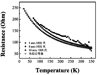
[0065] Its electrical properties are maintained at a low temperature of 20K for 10 hours without significant change, and its electrical properties can still be kept stable after being bent 8,000 times in an atmospheric environment.

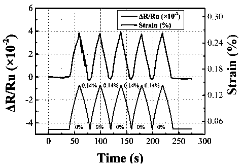
[0066] The stress sensing of the electronic skin is highly sensitive GF30.0. After 8000 bending-flattening cycles, the electrical resistance of the electronic skin still has no significant drift. The electronic skin has good recoverability. According to the test, the resistance of the electron...

Embodiment 3

[0068] An electronic skin, such as figure 1 As shown, including mica substrate 1, 50% Nb-doped BaTiO covered on the mica substrate 3 Semiconductor film layer 2, platinum electrode 3 covered on the semiconductor film layer, the thickness of the mica substrate is 20 μm, the thickness of the semiconductor film layer is 100 nm, the thickness of the platinum electrode is 80 nm, and the surface of the semiconductor film layer is an atomic agent flat surface .

[0069] Its electrical properties are maintained at a low temperature of 20K for 10 hours without significant change, and its electrical properties can still be kept stable after being bent 7,000 times in an atmospheric environment.

[0070] The stress sensing of the electronic skin is highly sensitive GF27.5. After 7000 bending-flattening cycles, the resistance of the electronic skin still has no significant drift. The electronic skin has good recoverability. According to the test, the resistance of the electronic skin rema...


PUM

PropertyMeasurementUnit
Thicknessaaaaaaaaaa
Thicknessaaaaaaaaaa
Thicknessaaaaaaaaaa

Abstract

The invention discloses an electronic skin and a preparation method thereof. The electronic skin includes a mica substrate, a 50% Nb-doped BaTiO3 semiconductor thin film layer covering the mica substrate, and a platinum electrode covering the semiconductor thin film layer, the thickness of the mica substrate is 0.02-20 [mu]m, the thickness of the semiconductor thin film layer is 5-200 nm, and thethickness of the metal electrode is 5-200 nm. The electronic skin can sense temperature, stress, deformation and light, has the advantages of flexible, low weight, low thickness, low power consumption, highly sensitive stress induction, low-temperature and organic solvent resistance and the like, and further has the characteristics of good low-temperature and flexural fatigue resistance; and the preparation process of electronic skin is simple, a mature coating process can be compatible with a semiconductor process, photoetching and ion etching can be realized, thus the efficiency is higher, device miniaturization and integration are more convenient, and industrialized promotion is easy.

Description

technical field [0001] The present invention relates to the technical field of electronic skin, more specifically, to an electronic skin and its preparation method and application. Background technique [0002] Electronic skin is an electronic sensor that can be bent or stretched, because it can detect stress, temperature, humidity, gas or light, etc., and it is as soft as skin and can be attached to the body of biology, robot, civil engineering or aircraft. The surface of the wing can also be implanted into clothes, gloves, and even bionic prosthetics and the body to make it feel tactile to the surrounding environment to form wearable, functional and certain sensing electronic devices. These characteristics make the electronic skin have great application significance in the fields of human-computer interaction, robot engineering and biomedical devices. [0003] For a long time, people's research on electronic skin has mostly used metal or silicon nanowires, carbon nanotube...

Claims


Application Information

Patent Timeline
IPC IPC(8): A61F2/10
CPCA61F2/105
Inventor 陆旭兵杨成郭敏
Owner INT ACAD OF OPTOELECTRONICS AT ZHAOQING SOUTH CHINA NORMAL UNIV
Why Eureka
Try Eureka