Preparation method for porous silicon/ZnO nanorod composite photo-anode

A technology of porous silicon and nanorods is applied in the field of preparation of porous silicon/ZnO nanorod composite photoanode, and achieves the effects of easy availability of raw materials, simple preparation method and improved absorption.

Inactive Publication Date: 2019-04-05
DONGHUA UNIV
View PDF4 Cites 5 Cited by
  • Summary
  • Abstract
  • Description
  • Claims
  • Application Information

AI Technical Summary

Problems solved by technology

[0006] The technical problem to be solved by the present invention is to provide a method for preparing a porous silicon / ZnO nanorod composite photoanode, which overcomes the defect that the existing photoanode needs to grow ZnO seed crystals before growing ZnO nanorods on the substrate

Method used


Image

  • Preparation method for porous silicon/ZnO nanorod composite photo-anode
  • Preparation method for porous silicon/ZnO nanorod composite photo-anode
  • Preparation method for porous silicon/ZnO nanorod composite photo-anode

Examples


Embodiment 1

[0027] (1) Polycrystalline silicon is etched by metal-assisted wet method to obtain porous silicon; the porous silicon substrate is ultrasonically washed in acetone, absolute ethanol, and deionized water in sequence, and 0.1580 g of potassium permanganate is added to 100 ml of water to form a 0.01 mol / L uniform solution, then put the porous silicon into the solution for 30 minutes and then clean it.

[0028] (2) Add 1.4875 g of zinc nitrate hexahydrate to 100 ml of water to form a uniform solution of 0.05 mol / L, then add 0.7009 g of hexamethylenetetramine and stir to form a mixed uniform solution.

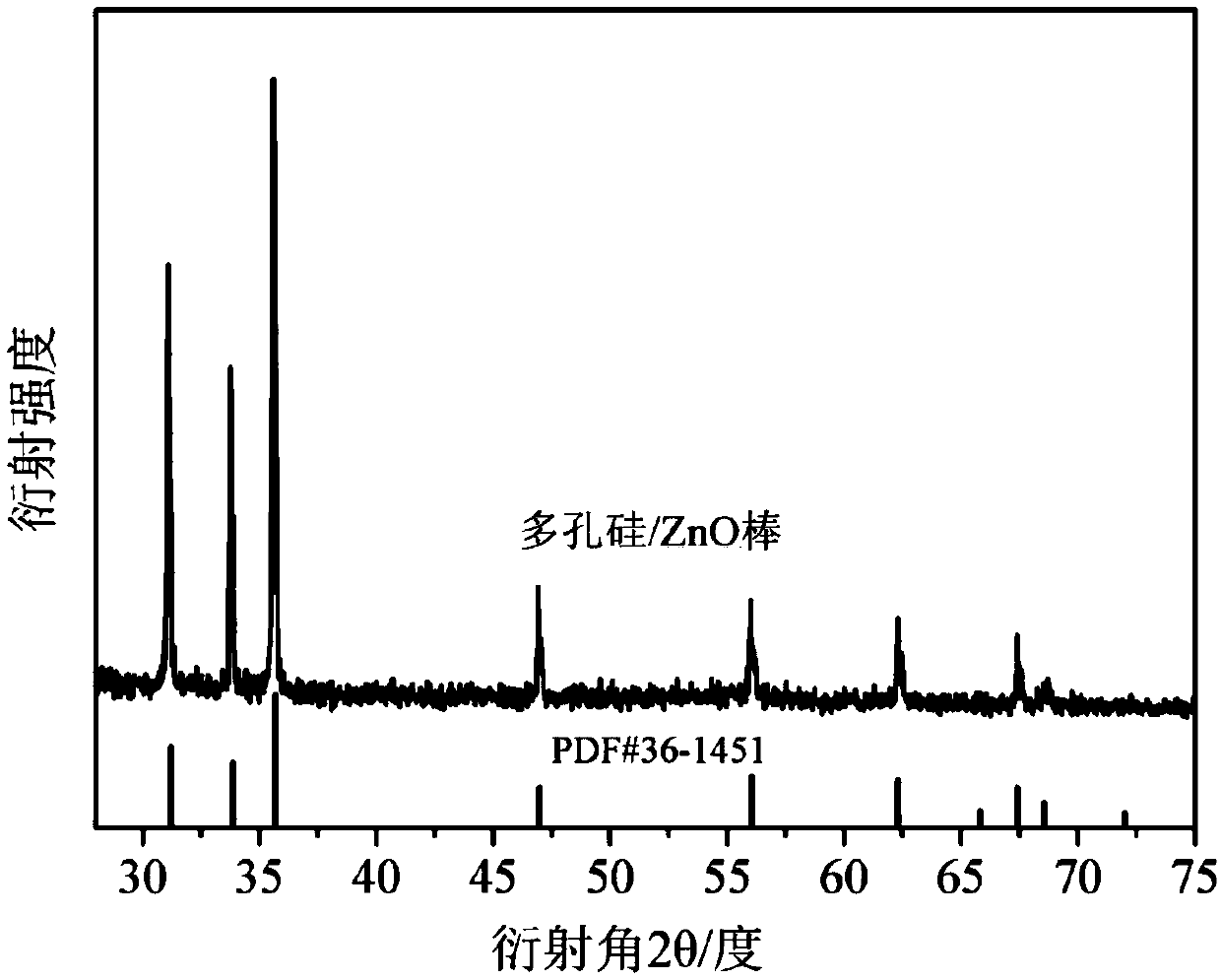
[0029] (3) Vertically immerse the porous silicon in step (1) into the mixed solution of step (2), and react in a water bath at 90°C for 2 hours. After the reaction, wash the porous silicon with deionized water and dry it to obtain porous silicon / ZnO nanometer Rod composite photoanode.

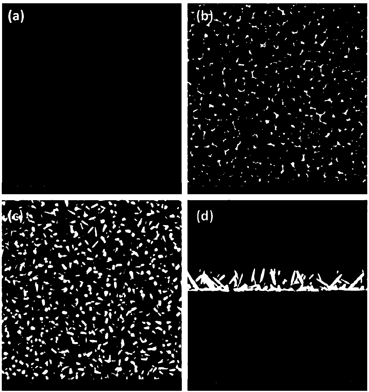
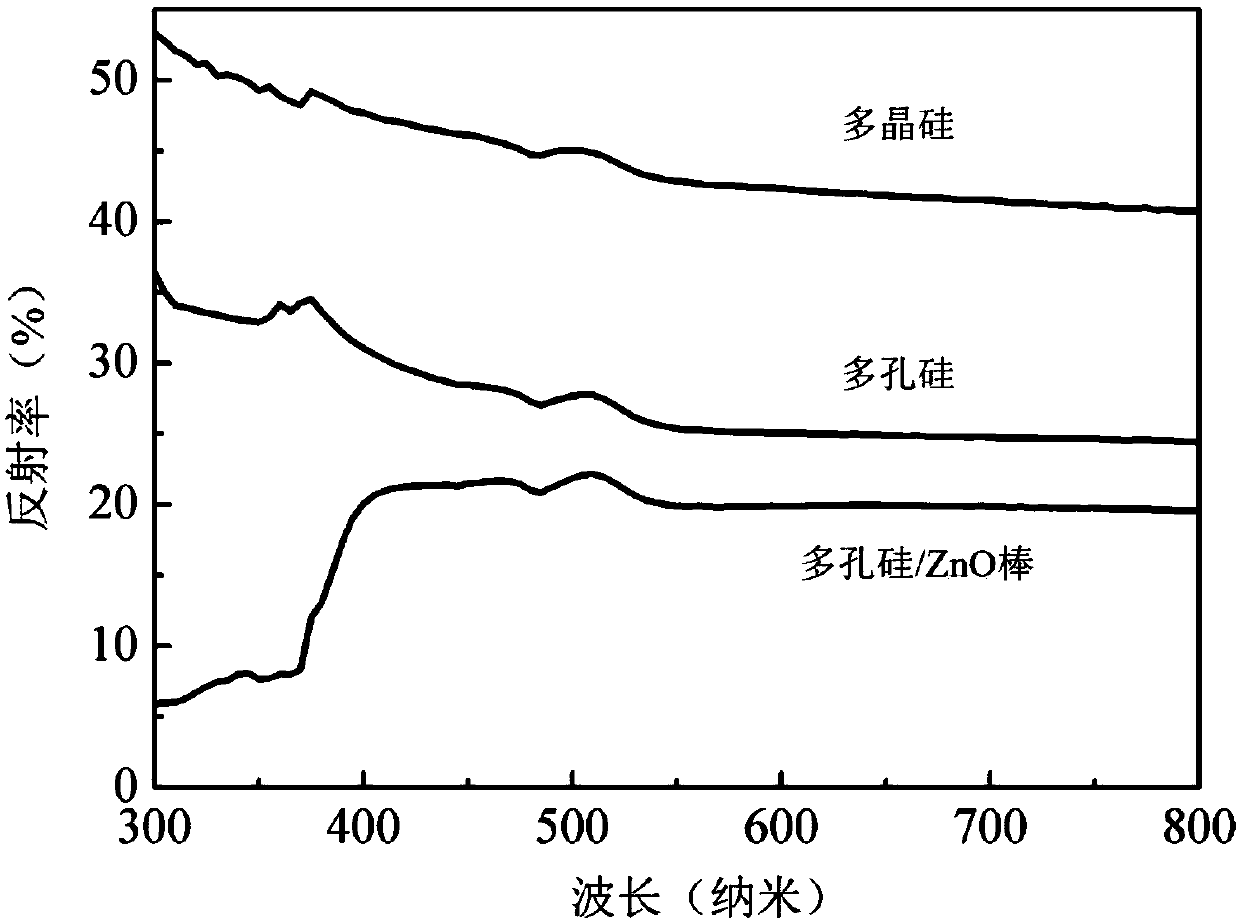
[0030] The SEM photos of polysilicon in this embodiment before and after metal-assisted wet et...

Embodiment 2

[0036] (1) Polycrystalline silicon is etched by metal-assisted wet method to obtain porous silicon; the porous silicon substrate is ultrasonically washed in acetone, absolute ethanol, and deionized water in sequence, and 1.5803 potassium permanganate is added to 100ml of water to form a 0.1mol / L homogeneous solution, then put the porous silicon into the solution for 20min and then clean it.

[0037] (2) Add 0.2975g of zinc nitrate hexahydrate to 100ml of water to form a uniform solution of 0.01mol / L, then add 0.1402g of hexamethylenetetramine and stir to form a mixed uniform solution.

[0038] (3) Vertically immerse the porous silicon of step (1) into the mixed solution of step (2), and react in a water bath at 70°C for 6 hours. After the reaction, the porous silicon is washed with deionized water and dried to obtain porous silicon / ZnO nanometer Rod composite photoanode.

[0039] The sample of this embodiment is used as the working electrode, the Pt sheet is used as the coun...

Embodiment 3

[0041] (1) Polysilicon is etched by metal-assisted wet method to obtain porous silicon; the porous silicon substrate is ultrasonically washed in acetone, absolute ethanol, and deionized water in sequence. Add 0.0790g of potassium permanganate into 100ml of water to form a uniform solution of 0.005mol / L, then put the porous silicon into the solution for 40min and then clean it.

[0042] (2) Add 5.9500 g of zinc nitrate hexahydrate to 100 ml of water to form a uniform solution of 0.2 mol / L, then add 2.8036 g of hexamethylenetetramine and stir to form a mixed uniform solution.

[0043](3) Vertically immerse the porous silicon in step (1) into the above solution, and react in a water bath at 95° C. for 1 h. After the reaction, the porous silicon was washed with deionized water and dried to obtain a porous silicon / ZnO nanorod composite photoanode.

[0044] The sample of this embodiment is used as the working electrode, the Pt sheet is used as the counter electrode, the saturated c...


PUM

PropertyMeasurementUnit
lengthaaaaaaaaaa
diameteraaaaaaaaaa
pore sizeaaaaaaaaaa

Abstract

The invention relates to a preparation method for a porous silicon/ZnO nanorod composite photo-anode. The preparation method comprises the following steps: (1) ultrasonic-washing a porous silicon substrate successively in acetone, absolute ethyl alcohol and deionized water, and treating by using potassium permanganate solution, washing, to obtain the completely washed porous silicon substrate; (2)preparing uniform aqueous solution of zinc nitrate hexahydrate, adding hexamine, stirring, to obtain uniformly mixed solution; and (3) enabling the porous silicon substrate to be vertically immergedin the mixed solution, performing a water bath reaction, washing, and airing, to obtain the porous silicon/ZnO nanorod composite photo-anode. The preparation method is simple, and low in cost. A ZnO seed crystal is not needed, and porous silicon is selected as the substrate. An obtained sample has very high light current density.

Description

technical field [0001] The invention belongs to the technical field of photoelectric catalysis, and in particular relates to a method for preparing a porous silicon / ZnO nanorod composite photoanode. Background technique [0002] In today's world, the problems of environmental pollution and energy shortage are increasing day by day. Although the existing technology and non-renewable energy can meet the population growth and economic development of human beings for hundreds of years, the corresponding social consequences are very severe. Photoelectrocatalytic technology can degrade organic pollutants under the irradiation of sunlight and a certain bias voltage, and can also generate clean energy hydrogen, which is an ideal technology to solve environmental pollution and energy shortage. [0003] In photocatalytic systems, silicon wafers are often used as conductive substrates, but crystalline silicon itself has defects as a conductive substrate. First, about 30% of incident p...

Claims


Application Information

Patent Timeline
Patent Type & Authority Applications(China)
IPC IPC(8): B01J23/06
CPCB01J23/06
Inventor 张青红孟颖王宏志李耀刚侯成义
Owner DONGHUA UNIV
Why Eureka
Try Eureka