Photoelectrochemical mechanical polishing processing method of semiconductor wafer

A mechanical polishing and photoelectrochemical technology, applied in semiconductor/solid-state device manufacturing, metal processing equipment, grinding/polishing equipment, etc., can solve the problems of long processing time, high cost, low polishing removal rate, etc. The processing device is simple, the polishing removal rate is fast, and the processing method is easy to achieve.

Active Publication Date: 2019-04-19
XIAMEN UNIV
View PDF10 Cites 10 Cited by
  • Summary
  • Abstract
  • Description
  • Claims
  • Application Information

AI Technical Summary

Problems solved by technology

[0004] It can be seen that in the process of removing subsurface damage by traditional CMP, the extremely high chemical inertness of ...

Method used


Image

  • Photoelectrochemical mechanical polishing processing method of semiconductor wafer
  • Photoelectrochemical mechanical polishing processing method of semiconductor wafer
  • Photoelectrochemical mechanical polishing processing method of semiconductor wafer

Examples


Embodiment Construction

[0057] The present invention will be further described below in conjunction with accompanying drawing.

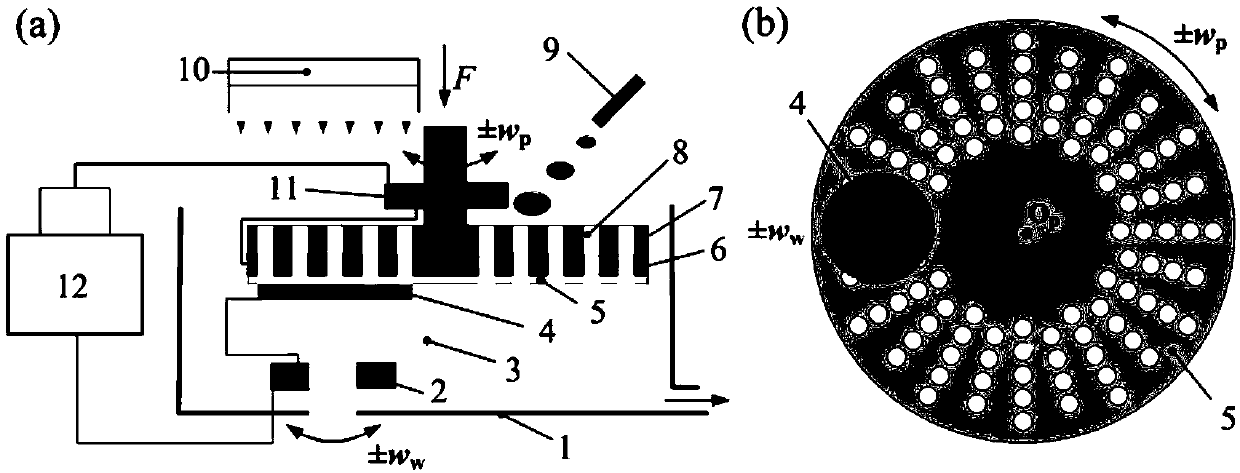
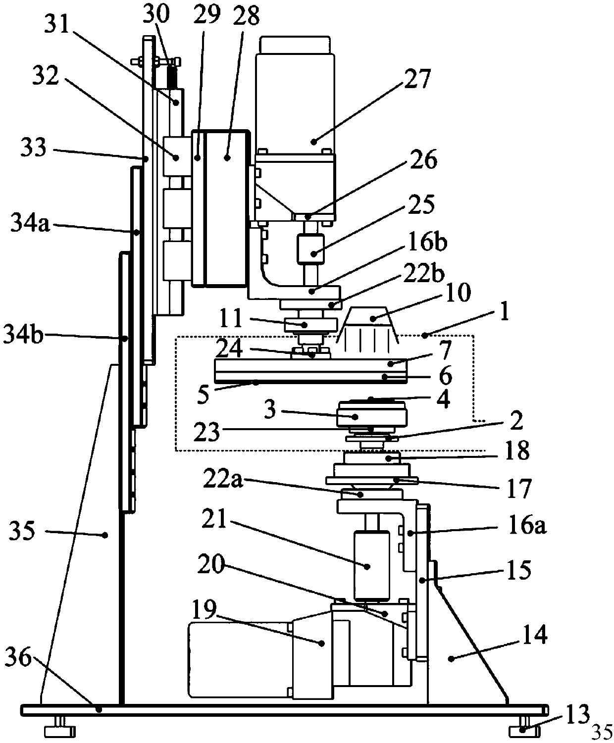
[0058] (1) Fix the wafer on the polishing head, and after being driven, the wafer rotates axially with the polishing head; the wafer is connected to the metal part of the polishing head through conductive glue, and the polishing head is connected to the inner ring wire of the conductive slip ring, and then connected to the conductive The outer ring of the slip ring is connected to form a passage;

[0059] (2) Bond the polishing pad to the counter electrode disc, and the counter electrode disc is fixed on the polishing disc. After driving, the polishing pad contacts the surface of the wafer and generates relative movement. The counter electrode disc can be connected to the inner ring wire of the conductive slip ring. Connect, and then connect with the outer ring wire to form a path;

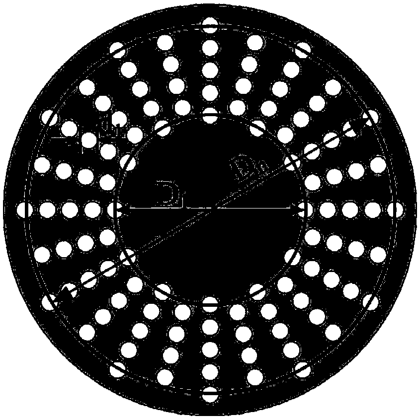
[0060] (3) Through holes are processed on the counter electrode disc and the polishing dis...


PUM


Abstract

The invention discloses a photoelectrochemical mechanical polishing processing method of a semiconductor wafer and a processing device. The method comprises the following steps that the wafer is fixedon a polishing head through a conductive adhesive in a bonding mode, and the wafer is connected to the positive electrode of an external power supply through leads of an inner ring and an outer ringof a conductive slip ring below the wafer; a polishing pad is adhered to the bottom of a counter electrode plate, the counter electrode plate is fixed at the bottom of a polishing plate, a through hole is formed in the position, corresponding to the polishing plate, of the counter electrode plate, and the counter electrode plate is connected to the negative electrode of the external power supply through the leads of the inner ring and the outer ring of the conductive slip ring above the counter electrode plate; and ultraviolet light emitted by an ultraviolet light source can irradiate the surface of the wafer through the through hole, and polishing solution can also be jetted into the through hole to be entered the contact area of the wafer and the polishing pad. The photoelectrochemical mechanical polishing processing device can well realize the processing method involved in the invention, and the processing device has the advantages that the operation is simple, the implementation iseasy, and the process parameters can be flexibly adjusted; and effects of being rapid in the removal rate and good in the processed surface quality can be obtained in actual processing of the galliumnitride wafers.

Description

technical field [0001] The invention relates to the technical field of polishing processing, more specifically to a photoelectrochemical mechanical polishing processing method of a semiconductor wafer. Background technique [0002] The third-generation semiconductor representative materials represented by gallium nitride (GaN), silicon carbide (SiC), and diamond have high thermal conductivity, high breakdown electric field, high electron saturation rate and high radiation resistance. Compared with the previous generation of semiconductor materials, it is more suitable for the production of high-temperature, high-frequency, high-power, radiation-resistant high-power devices. [0003] When GaN and SiC crystal materials are used as devices, the materials are required to have high surface quality, no scratches, microcracks, low dislocations, residual stress and other surface / subsurface damage. However, GaN and SiC crystal materials have large bond energy, strong chemical inertn...

Claims


Application Information

Patent Timeline
IPC IPC(8): B24B37/10B24B37/04B24B7/22H01L21/02
CPCB24B7/228B24B37/042B24B37/044B24B37/046B24B37/10H01L21/02013
Inventor 时康康仁科欧李苇董志刚胡慧勤田中群
Owner XIAMEN UNIV
Why Eureka
Try Eureka