Non-junction dual-grid line tunneling field-effect transistor

A technology of tunneling field effect and double gate lines, which is applied in the direction of semiconductor devices, electrical components, circuits, etc., can solve the problems of small on-state current of devices and limited tunneling area, so as to increase the on-state current, enhance the electric field, The effect of increasing the tunneling area

Active Publication Date: 2019-05-14
UNIV OF ELECTRONICS SCI & TECH OF CHINA
View PDF2 Cites 2 Cited by
  • Summary
  • Abstract
  • Description
  • Claims
  • Application Information

AI Technical Summary

Problems solved by technology

However, the carrier tunneling of ordinary junctionless tunneling field-effect transistors occurs at the interface between the source-drain region and the channel region, and the tunneling area is limited, and the on-state current of the device is small; there...

Method used


Image

  • Non-junction dual-grid line tunneling field-effect transistor
  • Non-junction dual-grid line tunneling field-effect transistor
  • Non-junction dual-grid line tunneling field-effect transistor

Examples


Embodiment Construction

[0025] The present invention will be further described below in conjunction with the accompanying drawings and embodiments.

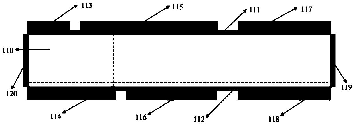
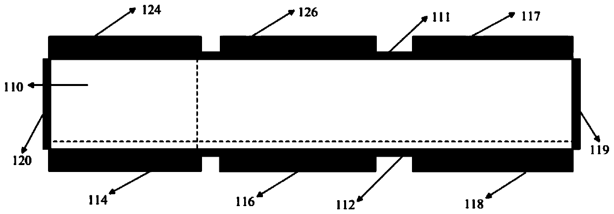
[0026] This embodiment provides a junctionless double gate line tunneling field effect transistor, the structure of which is as follows figure 1 As shown, it includes a channel region (110), an insulating layer, a source metal, a metal gate, a drain metal, a drain electrode (119) and a source electrode (120), wherein the insulating layer includes a top insulating layer (111) , a bottom insulating layer (112), the source metal includes a top source metal (113) and a bottom source metal (114), and the metal gate includes a top metal gate (115) and a bottom metal gate (116), so The drain metal includes the top drain metal (117) and the bottom drain metal (118); wherein,

[0027]The channel region is in the shape of a cuboid, the upper surface of the channel region is covered with a top insulating layer, the lower surface is covered with a bottom insulati...


PUM

PropertyMeasurementUnit
Thicknessaaaaaaaaaa
Thicknessaaaaaaaaaa

Abstract

The invention belongs to the field of semiconductor devices, and provides a non-junction dual-grid line tunneling field-effect transistor. The non-junction dual-grid line tunneling field-effect transistor is used for improving an on-state current of the non-junction dual-grid line tunneling field-effect transistor. In the tunneling field-effect transistor, P-type doping characteristic source region and an N-type doping characteristic drain region are formed in a non-doped or light-doped channel by electrical doping according to difference between a work function of source region metal and drain region metal and semiconductor electron affinity of a channel region, a vertical symmetric dual-grid structure of a traditional non-junction dual-grid tunneling transistor is changed, so that top-layer metal grid and bottom-layer metal grid are provided with an asymmetric dual-grid structure with length difference, carrier line tunneling is introduced to the non-junction dual-grid tunneling field-effect transistor, and line tunneling is taken as main; and meanwhile, by extending extension length of the top-layer metal grid, the length difference between the top-layer metal grid and the bottom-layer metal grid is increased by shortening the length of the bottom-layer metal grid, the line tunneling area of the transistor is expanded, the carrier tunneling probability is improved, and the on-state current of the device is effectively improved.

Description

technical field [0001] The invention belongs to the field of semiconductor devices and relates to a junctionless tunneling field effect transistor, in particular to a junctionless double gate line tunneling field effect transistor capable of effectively increasing the on-state current. Background technique [0002] With the advancement of integrated circuit technology, the core device in today's VLSI CMOS technology is still MOSFET (Metal-Oxide-Semiconductor Field-Effect Transistor). As the feature size of MOSFET continues to shrink, the short-channel effect brought Obviously, at the same time, due to the limitation of the working mechanism of MOSFET using carrier drift and diffusion, its subthreshold swing cannot be lower than 60mV / dec at room temperature, thus increasing part of the power consumption of the integrated circuit. [0003] In order to reduce the operating voltage of the device and thereby reduce the power consumption of the integrated circuit, it has become a ...

Claims


Application Information

Patent Timeline
IPC IPC(8): H01L29/739H01L29/417H01L29/423
Inventor 谢倩李杰黄安鹏王政
Owner UNIV OF ELECTRONICS SCI & TECH OF CHINA
Why Eureka
Try Eureka