N-doping SiC single crystal nanometer pore passage array and prepared photoelectric catalysis anode
A single crystal nanometer, photoelectric catalysis technology, applied in the direction of electrodes, single crystal growth, single crystal growth, etc., can solve the problems of difficult photocatalytic electrode preparation, poor light harvesting ability, small surface area, etc., and achieve high photoelectric catalysis current density , wide photoresponse, and high catalytic stability
- Summary
- Abstract
- Description
- Claims
- Application Information
AI Technical Summary
Problems solved by technology
Method used
Image
Examples
Embodiment 1
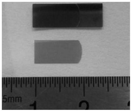
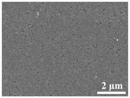
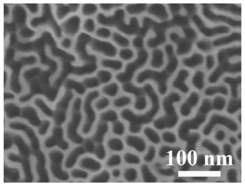
[0032] Cut the N-doped SiC single wafer into a size of 0.5 × 1.5 cm 2The SiC single wafer is 4H-SiC; the N-doped SiC small wafer is used as the anode, the graphite sheet is used as the cathode, and the mixed solution of hydrofluoric acid, ethanol and hydrogen peroxide at a ratio of 6:6:1 is used as the electrolyte , using anodic oxidation etching to obtain N-doped SiC single crystal nanopore arrays on the surface of SiC small wafers; coat a layer of conductive silver paste on the surface of conductive glass, and then use epoxy resin to seal the surrounding of the conductive silver paste film ; The N-doped SiC single crystal nanopore array film is peeled off from the surface of the SiC small wafer, and transferred to the surface of a conductive glass coated with a conductive silver paste, and the conductive glass is ITO. The physical picture of the SiC nanostructure etching film peeled off from the surface of the SiC small wafer made by this embodiment is as follows figure 1 a...
Embodiment 2
[0034] The only difference from Example 1 is that the electrolyte in this example is a mixed solution prepared with hydrofluoric acid, ethanol and hydrogen peroxide at a ratio of 6:6:1.05 in parts, and the others are the same as in Example 1. Let me repeat. The N-doped SiC single crystal nano-channel array photocatalytic anode prepared in Example 2 has a highly oriented, large-area, and uniform nano-channel array structure, and the wall thickness of the nano-channel is only 14 nm. The depth of the cross-section of the nanohole array prepared in this embodiment is about 18 μm.
Embodiment 3
[0036] The only difference from Example 1 is that the electrolyte in this example is a mixed solution prepared with hydrofluoric acid, ethanol and hydrogen peroxide at a ratio of 6:6:1.1 in parts, and the others are the same as in Example 1. Let me repeat. The N-doped SiC single crystal nanopore array photocatalytic anode prepared in Example 3 has a highly oriented, large-area, and uniform nanopore array structure, and the wall thickness of the nanopore is only 13 nm. The depth of the cross-section of the nanohole array prepared in this embodiment is about 19 μm.
PUM
| Property | Measurement | Unit |
|---|---|---|
| thickness | aaaaa | aaaaa |
| depth | aaaaa | aaaaa |
| depth | aaaaa | aaaaa |
Abstract
Description
Claims
Application Information


