Biosensing chip and preparation method and application thereof

A bio-sensing and chip technology, applied in the field of sensors, achieves strong adsorption efficiency, expands application scenarios, and is easy to achieve.

Active Publication Date: 2019-06-28
SHENZHEN UNIV
View PDF4 Cites 2 Cited by
  • Summary
  • Abstract
  • Description
  • Claims
  • Application Information

AI Technical Summary

Problems solved by technology

[0004] The purpose of the present invention is to overcome the deficiencies of the prior art, to provide a biosensor chip and its preparation method, to solve the technical problem that there is no visible light excitation biosensor

Method used


Image

  • Biosensing chip and preparation method and application thereof
  • Biosensing chip and preparation method and application thereof
  • Biosensing chip and preparation method and application thereof

Examples


preparation example Construction

[0036] Another aspect of the present invention provides a method for preparing the biosensor chip, comprising the steps of:

[0037] S01: Coating a layer of base film on one side of the prism;

[0038] S02: depositing a coupling layer on the base film;

[0039] S03: Finally, deposit a transfer layer on the surface of the coupling layer.

[0040] Specifically, in the step S01, a physical vapor deposition method may be used to vapor-deposit a metal thin film.

[0041] Specifically, in the step S02, a coupling layer may be deposited on the gold film by a plasma-enhanced chemical vapor deposition system.

[0042] Specifically, in the step S03, a transfer layer may be deposited on the surface of the coupling layer by chemical vapor deposition.

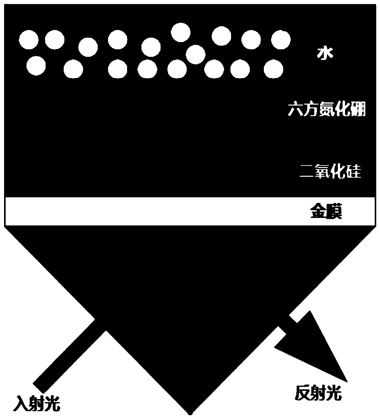
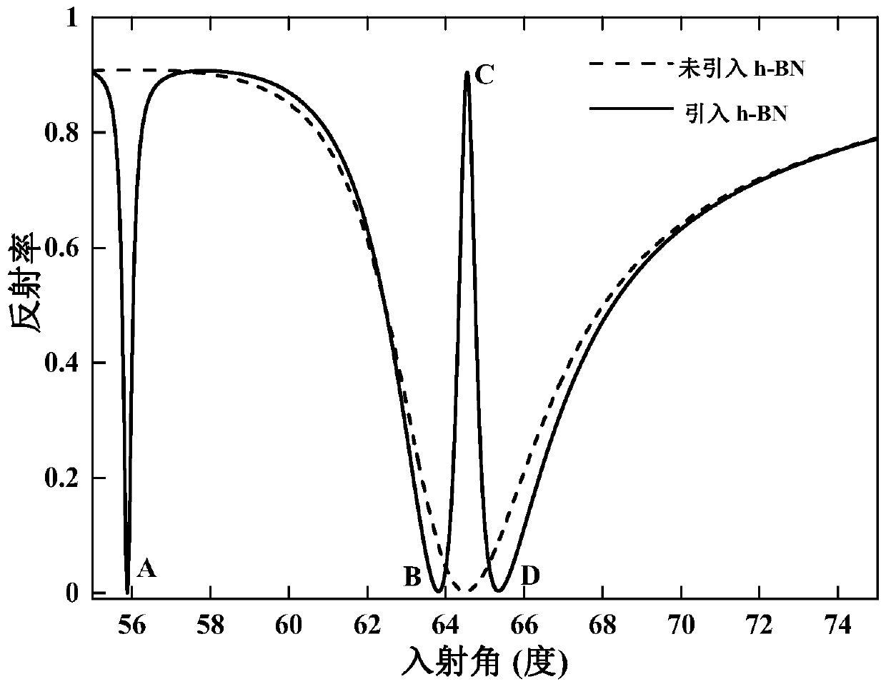
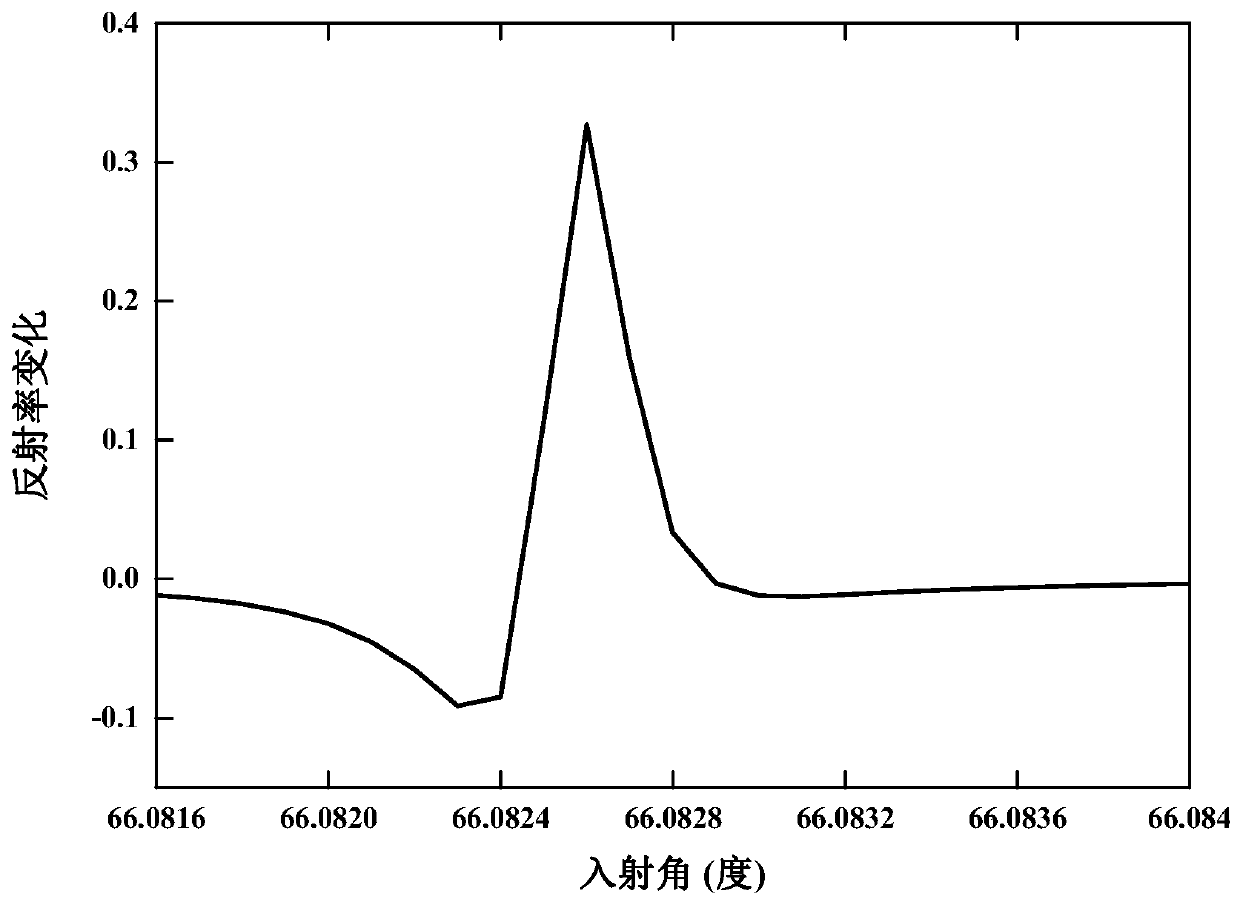
[0043] The invention utilizes the ultra-low plasmon loss characteristic of boron nitride to perform prism coupling test on the sensing chip. Since the two-dimensional structure material has the advantages of large surface area and many ...

Embodiment 1

[0045] The embodiment of the present invention provides a biosensor chip and a preparation method thereof.

[0046] The biosensor chip includes:

[0047] 48nm gold base film;

[0048] 450nm silica coupling layer;

[0049] 650nm hexagonal boron nitride thin film is passed to the layer.

[0050] Described preparation method comprises:

[0051] First, a metal film with a thickness of 48nm is evaporated on the SF11 or BK7 prism section by physical vapor deposition method;

[0052] Then silicon dioxide was deposited to a thickness of 450 nm on the gold film by a plasma enhanced chemical vapor deposition (PECVD) system.

[0053] Finally, a hexagonal boron nitride material with a thickness of 650 nm was deposited on the silicon dioxide surface by chemical vapor deposition (Chemical Vapor Deposition, CVD).

[0054] Example 1

[0055] The embodiment of the present invention provides a biosensor chip and a preparation method thereof.

[0056] The biosensor chip includes:

[0057...

Embodiment 2

[0068] The embodiment of the present invention provides a biosensor chip and a preparation method thereof.

[0069] The biosensor chip includes:

[0070] 45nm silver-based film;

[0071] 100nm silicon dioxide coupling layer;

[0072] 800nm ​​hexagonal boron nitride thin film is passed to the layer.

[0073] Described preparation method comprises:

[0074] First, a metal film with a thickness of 40nm is evaporated on the SF11 or BK7 prism section by physical vapor deposition method;

[0075] Silicon dioxide was then deposited on the gold film with a thickness of 100 nm by a plasma enhanced chemical vapor deposition (PECVD) system.

[0076] Finally, a hexagonal boron nitride material with a thickness of 800 nm was deposited on the silicon dioxide surface by chemical vapor deposition (Chemical Vapor Deposition, CVD).


PUM

PropertyMeasurementUnit
thicknessaaaaaaaaaa
thicknessaaaaaaaaaa
thicknessaaaaaaaaaa

Abstract

The invention provides a biosensing chip. The biosensing chip comprises a prism coupling structure, a basement membrane layer, a coupling layer and a conductive layer; the prism coupling structure, the basement membrane layer, the coupling layer and the conductive layer are orderly laminated and combined along a direction to the conductive layer from the coupling structure; the material of the conductive layer is hexagonal boron nitride; a top layer two-dimensional material boron nitride provides a light waveguide model; and the strong coupling of a plasma excimer mode and the light waveguidemode promotes the production of a Fano resonance narrow-line. On the one hand, the biosensing chip provided by the invention inherits ultra-high detection sensitivity and ultra-high detection precision; on the other hand, the excitation wavelength is located at a visible light area by adopting the hexagonal boron nitride, and an application scene and an excitation condition are broadened.

Description

technical field [0001] The invention belongs to the field of sensors, and in particular relates to a biological sensor chip. Background technique [0002] In recent years, the field of materials science has entered a stage of rapid development, especially the strong rise of emerging two-dimensional materials provides a new research idea for the design and development of new plasmonic sensor devices. Two-dimensional materials not only possess large molecular adsorption sites, but also exhibit some amazing physical, optical, electronic, plasmonic, and chemical properties. Although the hybrid structure formed by effectively integrating thin layers of two-dimensional materials and plasmonic metal films can produce significant sensitivity enhancement, the introduction of two-dimensional materials also reduces the detection accuracy of surface plasmon resonance sensing devices to a certain extent. The main reason is that the introduction of two-dimensional materials will signific...

Claims


Application Information

Patent Timeline
Patent Type & Authority Applications(China)
IPC IPC(8): G01N21/552
Inventor 袁玉峰彭晓宋军屈军乐
Owner SHENZHEN UNIV
Why Eureka
Try Eureka