Method for synthesizing polymeric microspheres
A technology for synthesizing polymers and polymer solutions, applied in the field of polymer microsphere preparation, can solve the problems of difficult size control, low reaction efficiency, back-locking of synthesis process steps, etc., achieves good molding state, simple preparation process, and is conducive to popularization applied effect
- Summary
- Abstract
- Description
- Claims
- Application Information
AI Technical Summary
Problems solved by technology
Method used
Image
Examples
Embodiment 1
[0038] The method for synthesizing polymer microspheres in this embodiment comprises the following steps:
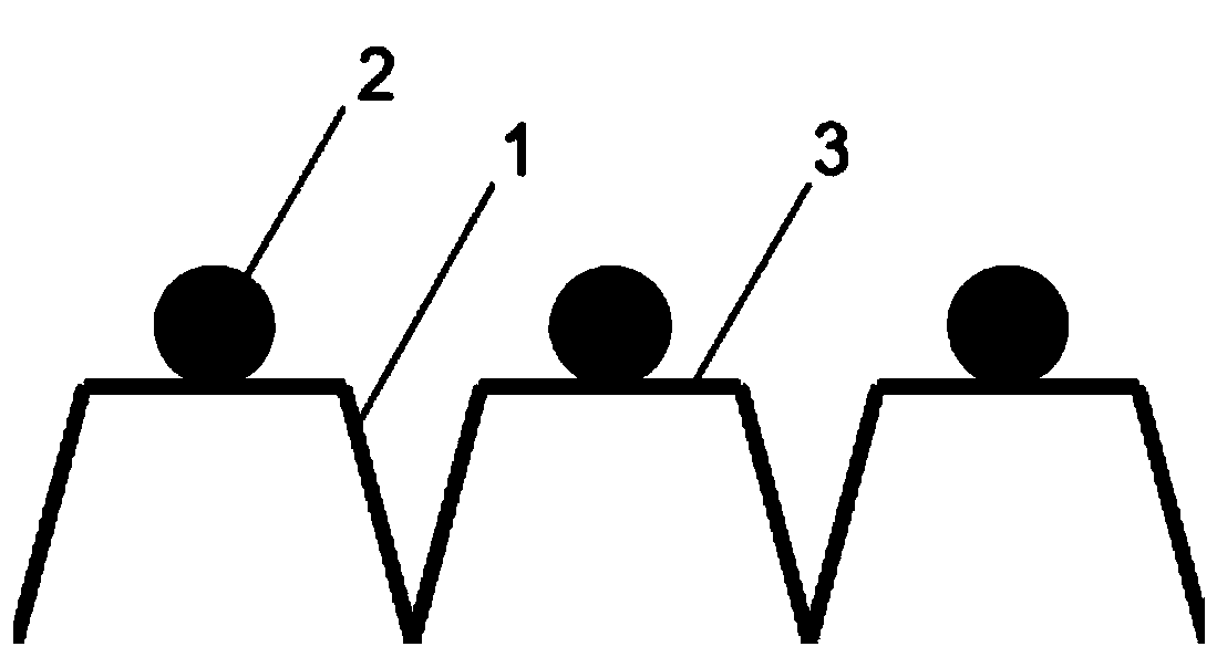
[0039] (1) Photolithography on the surface of the silicon wafer to obtain a microstructure with grooves and micro-platforms.
[0040] The silicon wafer was treated with plasma under vacuum condition for 25 minutes, and then the silicon wafer was heated at 300° C. for 25 minutes. Under the condition of yellow light irradiation, the photoresist is dropped on the surface of the silicon wafer with a thickness of 500um, an oxide layer thickness of 300nm, a crystal orientation of 100° and a diameter of 100mm, and then spin-coated, and the spin-coating acceleration is 750r / s 2 , the maximum speed is 3500r / s, then the silicon wafer is heated and solidified at 100°C, then the mask plate is exposed for 6s, and developed for 20s with a developer; the developer is 20wt% tetramethylammonium hydroxide solution and water according to 1: 7 volume ratio configuration.
[0041] The sili...
Embodiment 2
[0046] The method for synthesizing polymer microspheres in this embodiment comprises the following steps:
[0047] (1) Photolithography on the surface of the silicon wafer to obtain a microstructure with grooves and micro-platforms.
[0048] The silicon wafer was treated with plasma under vacuum for 35 minutes, and then the silicon wafer was heated at 250° C. for 35 minutes. Under the condition of yellow light irradiation, the photoresist is dropped on the surface of the silicon wafer with a thickness of 600um, an oxide layer thickness of 310nm, a crystal orientation of 100.5° and a diameter of 100.3mm, and then spin-coated, and the spin-coating acceleration is 850r / s 2 , the maximum speed is 3500r / s, then the silicon wafer is heated and solidified at 120°C, then the mask plate is exposed for 7s, and developed for 24s with a developer; the developer is 30wt% tetramethylammonium hydroxide solution and water according to 1: 9 volume ratio configuration.
[0049] The silicon wa...
Embodiment 3
[0054] The method for synthesizing polymer microspheres in this embodiment comprises the following steps:
[0055] (1) Photolithography on the surface of the silicon wafer to obtain a microstructure with grooves and micro-platforms.
[0056] The silicon wafer was treated with plasma under vacuum condition for 30 minutes, and then the silicon wafer was heated at 280° C. for 30 minutes. Under the condition of yellow light irradiation, the photoresist is dropped on the surface of the silicon wafer with a thickness of 400um, an oxide layer thickness of 290nm, a crystal orientation of 99.5° and a diameter of 99.7mm, and then spin-coated, and the spin-coating acceleration is 800r / s 2 , the maximum speed is 3500r / s, then the silicon wafer is heated and solidified at 110°C, then the mask plate is exposed for 7s, and developed for 22s with a developer; the developer is 25wt% tetramethylammonium hydroxide solution and water according to 1: The volume ratio of 8 is configured.
[0057]...
PUM
| Property | Measurement | Unit |
|---|---|---|
| thickness | aaaaa | aaaaa |
| thickness | aaaaa | aaaaa |
| diameter | aaaaa | aaaaa |
Abstract
Description
Claims
Application Information


